We continue to investigate external device interrupt routing setup in the x86 system.
In Part 1 (Interrupt controller evolution) we looked at the theory behind interrupt controllers and all the necessary terminology. In Part 2 (Linux kernel boot options) we looked at how in practice the OS chooses between different interrupt controllers. In this part we will investigate how the BIOS sets IRQ to the interrupt controllers routing in a chipset.
None of the modern BIOS developer companies (AwardBIOS/AMIBIOS/Insyde) open their source code. But luсkily there is coreboot — a project aimed at replacing proprietary BIOS with free firmware code. In its source code we'll see what is needed to setup the interrupt routing in a chipset.

Theory
To start let's review and expand our theoretical knowledge of the subject. In Part 1 we highlighted a common path of an interrupt from the external device for the PIC and APIC cases.
PIC:
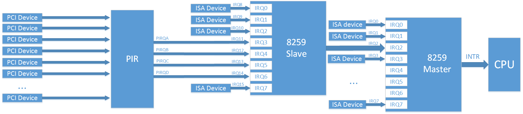
APIC:

On these pictures the mapping 'PCI device → PIR' is fairly abstract — it is actually a little bit more complicated. In reality every PCI device has four interrupt lanes (INTA#, INTB#, INTC#, INTD#). Also, every PCI device can have up to 8 so called 'functions' (which actually trigger interrupts) and each of these functions can connect to one of the INTx# lanes. Which INTx# interrupt will trigger each of the functions is either fixed in the hardware, or is defined by the device software configuration.
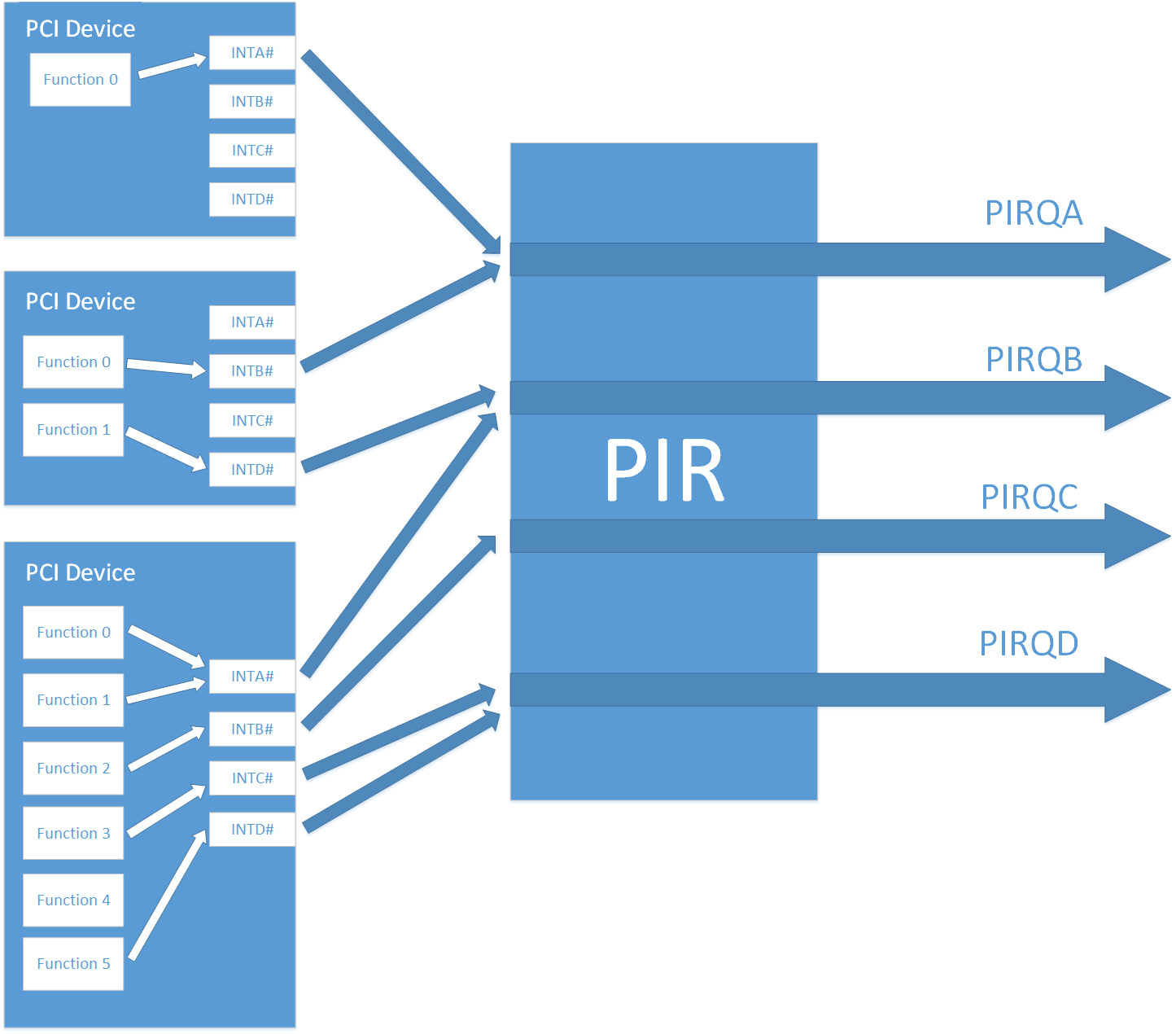
In a nutshell these functions are like separate logical blocks. For example, one PCI device can have in itself the 'SMBus controller' function, the 'SATA controller' function, and the 'LPC bridge' function. From the point of view of the OS every function is like a separate device with its own configuration space PCI Config.
In the most simple (and most common) case, a PCI device has only one function with its interrupt going to the lane INTA#. In general the device can have even more that 4 functions (as we've already said up to 8), and in this case it has to connect some of them to the same INTx# lane (PCI interrupts can share an interrupt lane). Also for PCI devices that are part of a chipset, by writing to its special registers it is usually possible to declare which functions use which INTx# lanes (or don't use them at all).
Summarizing all of that, let us write the complete path (routing) for an interrupt from any PCI function through INTx#→PIRQy→IRQz, where:
- INTx# — INT# lane (INTA#, INTB#, INTC#, INTD#) of the PCI device, which is used by a PCI function
- PIRQy — PIRQ lane (PIRQA, PIRQB, ...) from the PIR, which is connected with the INTx# lane
- IRQz — IRQ line (0, 1, 2, ...) from the interrupt controller (APIC/PIC), which is connected with the PIRQy lane
Why can't we just connect INTA#→PIRQA, INTB#→PIRQB,… everywhere?
Why should we waste our time paying attention to the interrupt routing setup? Suppose we've decided to not bother at all and have connected all the interrupt lanes from every PCI device to the PIRQ lanes in the same way. For example:
- INTA#→PIRQA
- INTB#→PIRQB
- INTC#→PIRQC
- INTD#→PIRQD
As we've already said above, the most common case is when a PCI device has only one function, and its interrupt is connected to the INTA# lane (because why would hardware device developer route it in a different way?). Therefore if we decided to route all lanes as we've written, almost all of the devices in a system would share interrupt lane PIRQA. Suppose this lane is connected to the IRQ16. This way, every time a processor has a signal that there is an interrupt on a IRQ16 line, it has to question all of the device drivers of the PCI devices connected to that IRQ16 line (PIRQA) if they have an interrupt. If there are many of those devices, it surely wouldn't increase system response to the interrupt. And in this case lanes PIRQB-PIRQD would stand idle wasted most of the time. Here is a picture that illustrates this problem:
Here is what it could be like:

This picture is a little bit complicated, but the point is that here we simply connect INTx# lanes with PIRQy lanes in a round-robin way (PIRQA, PIRQB, PIRQC, PIRQD, PIRQA, PIRQB, PIRQC, PIRQD, PIRQA, PIRQB, PIRQC, PIRQD, ...).
You should take into account that each PIRQ should have fairly the same number of PCI functions connected to it, and you should also consider that some functions trigger interrupts very rarely and some almost constantly (e.g. Ethernet controller). In this case even allocation of a separate PIRQ lane for such function may be completely justified.
From all of the above the BIOS developers have to balance PIRQ lanes with the interrupt load.
What should BIOS do anyway?
Here is a picture that summarizes the answer:

- 1) For every PCI function of every PCI device declare which INTx# the function triggers
For the external PCI devices you don't do any of this, but for the functions of PCI devices that are a part of the chipset you probably have to. - 2) For every PCI device set INTx#→PIRQy mapping
It is worthwhile to notice that it can be more than the standard 4 PIRQy signals (PIRQA, PIRQB, PIRQC, PIRQD). For example there can be 8 of them: PIRQA-PIRQH.
PIRQy signals go to IRQz lanes of the chosen interrupt controller (APIC/PIC). As we want to support all possible boot modes (take a look into Part 2 for that) it is necessary to fill both of these mappings:
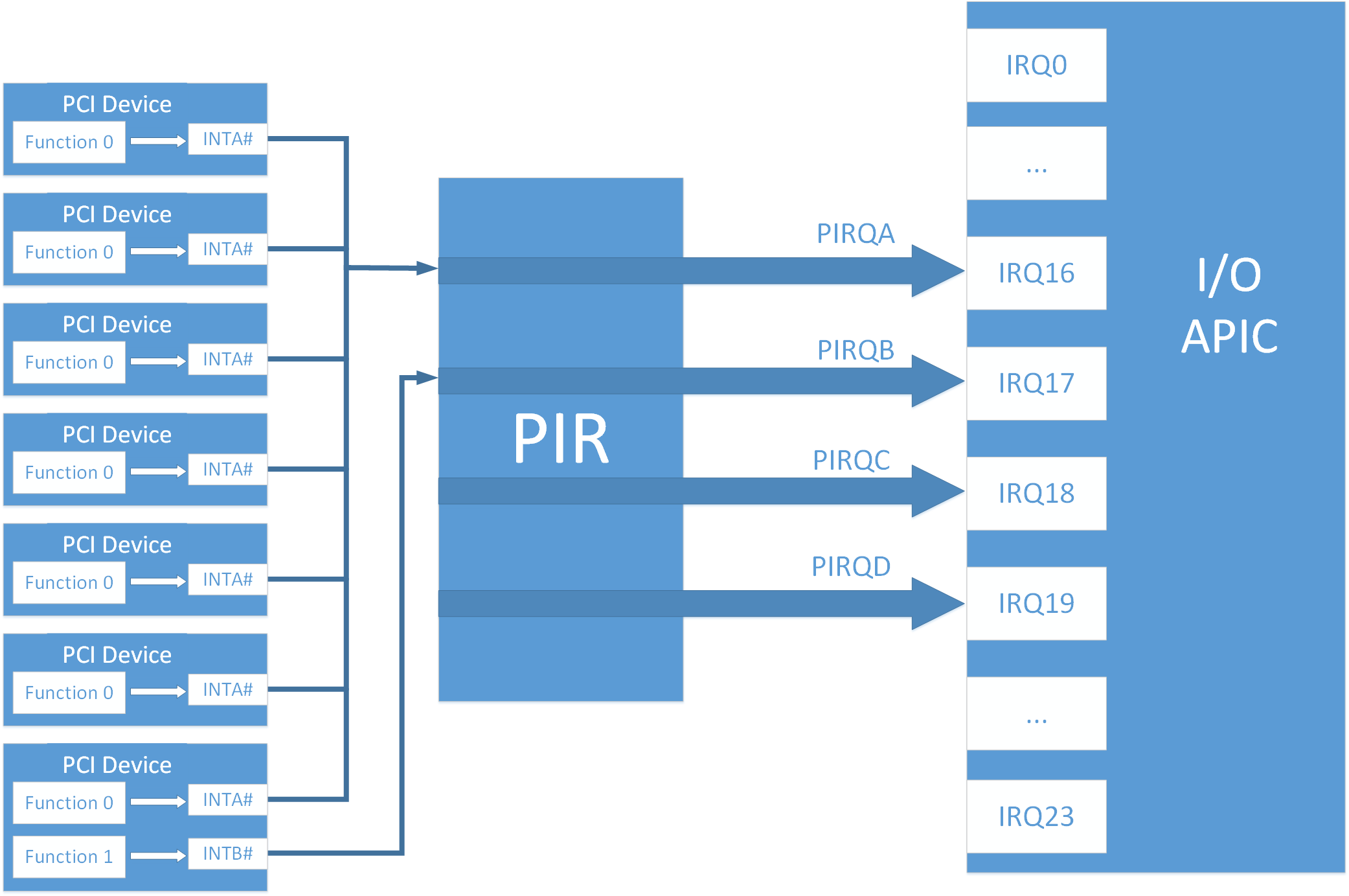
- 3a) Fill the mapping PIRQy→IRQz1 for the PIR→I/O APIC connection
Usually you don't have to do it, because in most cases the PIRQy lanes are hardwired to particular APIC lanes. The most common solution is PIRQA→IRQ16, PIRQB→IRQ17,… It is also the most simple one, because when we connect PIRQy lanes to the interrupt controller lanes ≥16, we don't have to worry about conflicts with non-shareable interrupts from ISA devices. - 3b) Fill the mapping PIRQy→IRQz2 for the PIR→PIC connection
This should be done if we want to support the case of routing through the PIC controller. There is no such obvious solution like in an APIC case, because with a PIC you should take into account the possibility of conflicts with non-shareable interrupts from ISA devices.
The next item that should be done is necessary to help the OS determine the routing mode. Hardware by itself usually doesn't use data from these registers:
- 4) Fill 'Interrupt Line/Interrupt Pin' registers for every PCI function
Actually the 'Interrupt Pin' register is usually filled automatically and in most cases is 'Read-Only', therefore it is probably only necessary to fill the 'Interrupt Line' register. It should be done when we use a routing through the PIC controller without giving the OS any interrupt routing table (again take a look into Part 2 for the explanation). If interrupt tables are present and this mapping is the same as the mapping in those tables ($PIR/ACPI), then the OS usually keeps it.
It is worthwhile to notice that we don't touch the topic of $PIR/MPtable/ACPI tables yet, we only look into how the registers of a chipset that are responsible for the interrupt routing should be configured before we handle execution to the OS bootloader. The interrupt tables are the subject of a separate article (which will probably be in the future).
So, all the theoretical ground is covered, let's go into practice!
Practice
As an example board in these articles I use custom motherboard with an Intel Haswell i7 CPU and LynxPoint-LP chipset. For this board I've ported and flashed coreboot with the SeaBIOS payload. Coreboot does all the necessary hardware-dependent initialization while its payload (SeaBIOS) provides the BIOS interface for the operating system. In this article I won't go into the coreboot configuration process, I will just try to show by example what settings the BIOS should do in a chipset for the correct IRQ interrupt routing from the external devices.
The coreboot project is actively developing, so to keep this article relevant, we will look at the source code for the last fixed version 4.9 (release 2018-12-20).
The motherboard that is the most similar to mine is a 'Google Beltino' with a 'Panther' variation. The main folder in the source code for this motherboard is «src\mainboard\google\beltino». Here are all the configuration settings and all of the specific code for this particular motherboard.
Now, let's find out where the configuration of all the things we have mentioned above is happening:
1) For every PCI function of every PCI device declare which INTx# the function triggers
This information is defined in the file «src/mainboard/google/beltino/romstage.c» in the structure 'rcba_config' through the 'DxxIP' registers (Device xx Interrupt Pin Register (IP)). This register shows to which of the INTx# (A/B/C/D) pins each PCI function connects its interrupt.
Possible choices are (see file «src/southbridge/intel/lynxpoint/pch.h»):
0h = No interrupt
1h = INTA#
2h = INTB#
3h = INTC#
4h = INTD#
It is possible that multiple functions would use the same pin.
It is allowed for a function to not use any interrupt pin at all ('No interrupt'). Everything is like as we saw on a picture in the beginning of the article.
The full code responsible for this paragraph is:
/* Device interrupt pin register (board specific) */
RCBA_SET_REG_32(D31IP, (INTC << D31IP_TTIP) | (NOINT << D31IP_SIP2) |
		(INTB << D31IP_SMIP) | (INTA << D31IP_SIP)),
RCBA_SET_REG_32(D29IP, (INTA << D29IP_E1P)),
RCBA_SET_REG_32(D28IP, (INTA << D28IP_P1IP) | (INTC << D28IP_P3IP) |
		(INTB << D28IP_P4IP)),
RCBA_SET_REG_32(D27IP, (INTA << D27IP_ZIP)),
RCBA_SET_REG_32(D26IP, (INTA << D26IP_E2P)),
RCBA_SET_REG_32(D22IP, (NOINT << D22IP_MEI1IP)),
RCBA_SET_REG_32(D20IP, (INTA << D20IP_XHCI)),
For better understanding let's look at a few examples:
Example 1:
In PCI device 0x1d (29 in decimal) there is one function (EHCI controller).
In this case we set its interrupt to INTA#.
00:1d.0 — INTA#
RCBA_SET_REG_32(D29IP, (INTA << D29IP_E1P)),Example 2:
In PCI device 0x1f (31 in decimal) there are several functions: Thermal Sensor controller (00:1f.6), SATA controller 2 (00:1f.2), SMBus controller (00:1f.3), SATA controller 1 (00:1f.2). We want to use SMBus controller, SATA controller 1, and Thermal Sensor controller only.
00:1f.2 - INTA# (SATA controller 1)
00:1f.3 - INTB# (SMBus controller)
00:1f.2 - No interrupt (SATA controller 2 is not used)
00:1f.6 - INTC# (Thermal Sensor controller)
For this configuration we should write:
RCBA_SET_REG_32(D31IP, (INTC << D31IP_TTIP) | (NOINT << D31IP_SIP2) | (INTB << D31IP_SMIP) | (INTA << D31IP_SIP)),Example 3:
One of the PCI devices has more than 4 functions that need to be enabled. In device 0x1c (decimal 28) every function is responsible for a particular PCI Express port. To enable ports 0-5 and to make the interrupts from them evenly balanced we can set it up like this:
00:1c.0 - INTA#	(PCI Express Port 0)
00.1c.1 - INTB#	(PCI Express Port 1)
00.1c.2 - INTC#	(PCI Express Port 2)
00.1c.3 - INTD#	(PCI Express Port 3)
00.1c.4 - INTA#	(PCI Express Port 4)
00.1c.5 - INTB#	(PCI Express Port 5)
00.1c.6 - No interrupt	(port is not used)
00.1c.7 - No interrupt	(port is not used)
RCBA_SET_REG_32(D28IP, (INTA << D28IP_P1IP) | (INTB << D28IP_P2IP) | (INTC << D28IP_P3IP) | (INTD << D28IP_P4IP) | (INTA << D28IP_P5IP) | (INTB << D28IP_P6IP) | (NOINT << D28IP_P7IP) | (NOINT << D28IP_P8IP)),2) For every PCI device set INTx#→PIRQy mapping
This information is also defined in the file «src\mainboard\google\beltino\romstage.c» in the 'rcba_config' structure, but in this case it is done through the 'DxxIR' registers (Device xx Interrupt Route Register).
Information in these registers shows to which PIRQy lane (A/B/C/D/E/F/G/H) each of the INTx# lanes is connected.
/* Device interrupt route registers */
RCBA_SET_REG_32(D31IR, DIR_ROUTE(PIRQG, PIRQC, PIRQB, PIRQA)),/* LPC */
RCBA_SET_REG_32(D29IR, DIR_ROUTE(PIRQD, PIRQD, PIRQD, PIRQD)),/* EHCI */
RCBA_SET_REG_32(D28IR, DIR_ROUTE(PIRQA, PIRQB, PIRQC, PIRQD)),/* PCIE */
RCBA_SET_REG_32(D27IR, DIR_ROUTE(PIRQG, PIRQG, PIRQG, PIRQG)),/* HDA */
RCBA_SET_REG_32(D22IR, DIR_ROUTE(PIRQA, PIRQA, PIRQA, PIRQA)),/* ME */
RCBA_SET_REG_32(D21IR, DIR_ROUTE(PIRQE, PIRQF, PIRQF, PIRQF)),/* SIO */
RCBA_SET_REG_32(D20IR, DIR_ROUTE(PIRQC, PIRQC, PIRQC, PIRQC)),/* XHCI */
RCBA_SET_REG_32(D23IR, DIR_ROUTE(PIRQH, PIRQH, PIRQH, PIRQH)),/* SDIO */
Example 1:
The PCI device 0x1c (28 in decimal) presents PCIe ports as we already know.
Let's make a direct connection:
- INTA#→PIRQA
- INTB#→PIRQB
- INTC#→PIRQC
- INTD#→PIRQD
RCBA_SET_REG_32(D28IR, DIR_ROUTE(PIRQA, PIRQB, PIRQC, PIRQD))Example 2:
The PCI device 0x1d (29 in decimal) has one function (EHCI controller) on its INTA# pin, the rest of the lanes are unused.
Connect lane INTA# with PIRQD:
RCBA_SET_REG_32(D29IR, DIR_ROUTE(PIRQD, PIRQD, PIRQD, PIRQD))In this case only the first record PIRQD (for INTA#) makes sense, the rest of them don't do anything useful.
3a) Fill the mapping PIRQy→IRQz1 for the PIR→I/O APIC connection
As we've already said, this mapping is usually fixed in the hardware, and this case is not an exception.
- PIRQA→IRQ16
- PIRQB→IRQ17
- ...
- PIRQH→IRQ23
3b) Fill the mapping PIRQy→IRQz2 for the PIR→PIC connection
In coreboot the content for these registers is defined in the file devicetree.cb in the motherboard folder «src\mainboard\google\beltino\».
'devicetree.cb' (the name 'devicetree' comes from the similar concept in the Linux kernel, and «cb» is an abbreviation for the word «coreboot») is a special file declaring configurations of a particular motherboard such as: which processor is used, which chipset is used, which devices are enabled in the chipset and which are not, and so on. In addition to that this file could contain some special information about chipset configuration. This is exactly what we need in this case:
register "pirqa_routing" = "0x8b"
register "pirqb_routing" = "0x8a"
register "pirqc_routing" = "0x8b"
register "pirqd_routing" = "0x8b"
register "pirqe_routing" = "0x80"
register "pirqf_routing" = "0x80"
register "pirqg_routing" = "0x80"
register "pirqh_routing" = "0x80"
These strings define PIRQy→IRQz2 mapping. In the code, after 'devicetree.cb' file parsing they would transform into variables «config->pirqX_routing».
The assignment «config->pirqa_routing = 0x8b» will mean that PIRQA is connected to IRQ11 lane (0x0b = 11) of the PIC controller, but the most significant bit (which is 0x80) means that interrupt routing is not active. To be honest, for me this seems like a mistake — by default PIC routing should be enabled, since the operating system can change to I/O APIC use by itself by setting this bit to 1 if it is necessary.
Therefore in this case it seems more correct to write:
register "pirqa_routing" = "0x0b"
register "pirqb_routing" = "0x0a"
register "pirqc_routing" = "0x0b"
register "pirqd_routing" = "0x0b"
register "pirqe_routing" = "0x80"	# not used
register "pirqf_routing" = "0x80"	# not used
register "pirqg_routing" = "0x80"	# not used
register "pirqh_routing" = "0x80"	# not used
We didn't enable the last 4 interrupts, because IRQ0 is always used for the system timer and surely can't be used (see General IBM-PC Compatible Interrupt Information).
But if we look carefully at paragraph '2)', we see that some PCI devices use PIRQE-PIRQH lanes, therefore keeping them unconnected is a right path to non-working devices.
So it is better to write something like this:
register "pirqa_routing" = "0x03"
register "pirqb_routing" = "0x04"
register "pirqc_routing" = "0x05"
register "pirqd_routing" = "0x06"
register "pirqe_routing" = "0x0a"
register "pirqf_routing" = "0x0b"
register "pirqg_routing" = "0x0e"
register "pirqh_routing" = "0x0f"
Actual filling of the corresponding device registers happens in the file src\southbridge\intel\lynxpoint\lpc.c in the function 'pch_pirq_init'.
The code fragment that is responsible for the register setting is:
/* Get the chip configuration */
config_t *config = dev->chip_info;
pci_write_config8(dev, PIRQA_ROUT, config->pirqa_routing);
pci_write_config8(dev, PIRQB_ROUT, config->pirqb_routing);
pci_write_config8(dev, PIRQC_ROUT, config->pirqc_routing);
pci_write_config8(dev, PIRQD_ROUT, config->pirqd_routing);

pci_write_config8(dev, PIRQE_ROUT, config->pirqe_routing);
pci_write_config8(dev, PIRQF_ROUT, config->pirqf_routing);
pci_write_config8(dev, PIRQG_ROUT, config->pirqg_routing);
pci_write_config8(dev, PIRQH_ROUT, config->pirqh_routing);
The address constants are defined in the same file pch.h
#define PIRQA_ROUT		0x60
#define PIRQB_ROUT		0x61
#define PIRQC_ROUT		0x62
#define PIRQD_ROUT		0x63
#define PIRQE_ROUT		0x68
#define PIRQF_ROUT		0x69
#define PIRQG_ROUT		0x6A
#define PIRQH_ROUT		0x6B
PIRQy→IRQz2 mapping for this particular chipset is written in PCI device LPC (address 00:1f.0) into the registers PIRQy_ROUT. It should be taken into account that usually not all the lanes IRQz2 on the PIC are permitted for use, but only part of them (e.g. 3,4,5,6,7,9,10,11,12,14,15). In a description for these registers there should be information about which IRQs are available for the connection of PIRQ lanes to them. So the proposed above mapping is possible only if a connection of PIRQ is possible to the lanes IRQ3, IRQ4, IRQ5, IRQ6, IRQ10, IRQ11, IRQ14, IRQ15. But if we look closely to the comment above the function 'pch_pirq_init', we see that this is the exact situation:
/* PIRQ[n]_ROUT[3:0] - PIRQ Routing Control
 * 0x00 - 0000 = Reserved
 * 0x01 - 0001 = Reserved
 * 0x02 - 0010 = Reserved
 * 0x03 - 0011 = IRQ3
 * 0x04 - 0100 = IRQ4
 * 0x05 - 0101 = IRQ5
 * 0x06 - 0110 = IRQ6
 * 0x07 - 0111 = IRQ7
 * 0x08 - 1000 = Reserved
 * 0x09 - 1001 = IRQ9
 * 0x0A - 1010 = IRQ10
 * 0x0B - 1011 = IRQ11
 * 0x0C - 1100 = IRQ12
 * 0x0D - 1101 = Reserved
 * 0x0E - 1110 = IRQ14
 * 0x0F - 1111 = IRQ15
 * PIRQ[n]_ROUT[7] - PIRQ Routing Control
 * 0x80 - The PIRQ is not routed.
 */
4) Fill 'Interrupt Line/Interrupt Pin' registers for every PCI function
There are 2 registers in a PCI config space (which every PCI function has by the PCI standard) that we are interested in:
- 3Ch: Interrupt Line — here we should write 'IRQz2' (number from 0 to 15), the number of an interrupt which eventually triggers the PIC controller when it is used
- 3Dh: Interrupt Pin — shows which INTx# lane (A/B/C/D) PCI function uses
Let's start from the latter. The 'Interrupt Pin' register would be filled automatically from the settings of the chipset (registers 'DxxIP') that we made in paragraph 1. We can't even explicitly rewrite these PCI registers, they are 'Read-Only' for the code.
So the only thing that is left for us to do is to fill the 'Interrupt Line' register with an IRQz2 interrupt for every PCI function.
If we know the mapping PIRQy→IRQz2 (paragraph 3b), and a mapping INTx#→PIRQy (paragraph 2) we could easily fill the 'Interrupt Line' register for every PCI function, knowing which interrupt INTx# it actually uses (paragraph 1).
In coreboot, 'Interrupt Line' registers are filled in the same file src\southbridge\intel\lynxpoint\lpc.c of the same 'pch_pirq_init' function:
/* Eric Biederman once said we should let the OS do this.
 * I am not so sure anymore he was right.
 */

for (irq_dev = all_devices; irq_dev; irq_dev = irq_dev->next) {
	u8 int_pin=0, int_line=0;

	if (!irq_dev->enabled || irq_dev->path.type != DEVICE_PATH_PCI)
		continue;

	int_pin = pci_read_config8(irq_dev, PCI_INTERRUPT_PIN);

	switch (int_pin) {
	case 1: /* INTA# */ int_line = config->pirqa_routing; break;
	case 2: /* INTB# */ int_line = config->pirqb_routing; break;
	case 3: /* INTC# */ int_line = config->pirqc_routing; break;
	case 4: /* INTD# */ int_line = config->pirqd_routing; break;
	}

	if (!int_line)
		continue;

	pci_write_config8(irq_dev, PCI_INTERRUPT_LINE, int_line);
}
This code for some reason implies that the mapping in any case should be INTA#→PIRQA, INTB#→PIRQB, INTC#→PIRQC, INTD#→PIRQD. But as we've seen earlier this easily could be done in a different way (see paragraph 2).
So it seems like «Eric Biederman once said» and we've copy-pasted it everywhere:
$ grep "Eric Biederman once said" -r src/
src/southbridge/intel/fsp_bd82x6x/lpc.c:        /* Eric Biederman once said we should let the OS do this.
src/southbridge/intel/i82801gx/lpc.c:   /* Eric Biederman once said we should let the OS do this.
src/southbridge/intel/i82801ix/lpc.c:   /* Eric Biederman once said we should let the OS do this.
src/southbridge/intel/lynxpoint/lpc.c:  /* Eric Biederman once said we should let the OS do this.
src/southbridge/intel/sch/lpc.c:        /* Eric Biederman once said we should let the OS do this.
In general coreboot doesn't pay much attention to legacy interrupt modes support. So you shouldn't be very surprised by this situation. It wouldn't prevent modern OS from booting, but if you ever decide to boot Linux with options like «acpi=off nolapic», it probably wouldn't be possible.
Conclusion
In conclusion let's repeat the typical information that is needed to be configured in a chipset to set PCI interrupt routing:
- For every PCI function of every PCI device declare which INTx# the function triggers
- For every PCI device set INTx#→PIRQy mapping
- Fill the mapping PIRQy→IRQz1 (PIR→APIC) and a mapping PIRQy→IRQz2 (PIR→PIC)
- Fill 'Interrupt Line/Interrupt Pin' registers for every PCI function.
Acknowledgments
Special thanks to Jacob Garber from the coreboot community for helping me with this article translation
