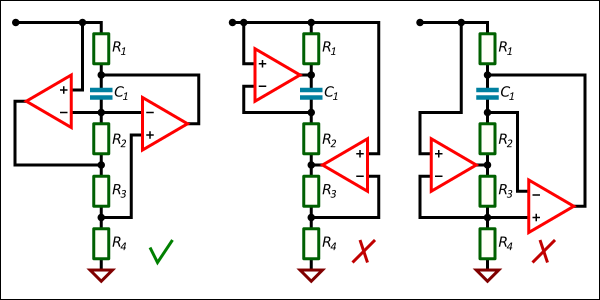
Gyrators are impedance converters usually used to simulate inductance in circuits. Though they are rarely used in discrete electronics, they are interesting circuits looking like pole dancers in pictures. There are studies on gyrators, but still something is missing, so it is interesting to do another one.
Quick test
Let’s start with simulating, set equal component values in different circuits taken from [1] and [3]. All Op Amps with maximum gain of 80 dB and Gain-Bandwidth product (GBW) of 10 MHz.
- Ideal inductor;
- Brugler, Fig. 4.11 in [1];
- Riordan 1, Fig. 4.15 in [1];
- Riordan 2, Fig. 4.16 in [1];
- Deboo, Fig. 4.19 in [1];
- Petin, [3];
- Antoniou 1, Fig. 4.20 in [1];
- Antoniou 2, Fig 4.21 in [1];
- Antoniou 3, Fig. 4.23 in [1];
- Antoniou 4, Fig. 4.25 in [1];
- Antoniou 5, Fig. 4.26 in [1];
- Antoniou 6, Fig 4.28 in [1];
- Modified Brugler, Fig. 4.30 in [1];
- Modified Deboo, Fig. 4.32 in [1];
- Modified Riordan 1, Fig. 4.34 in [1];
- Modified Riordan 2, Fig. 4.36 in [1];
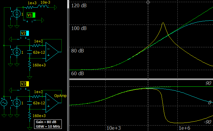
- Frequency response of the internally compensated 80 dB 10 MHz Op Amp;
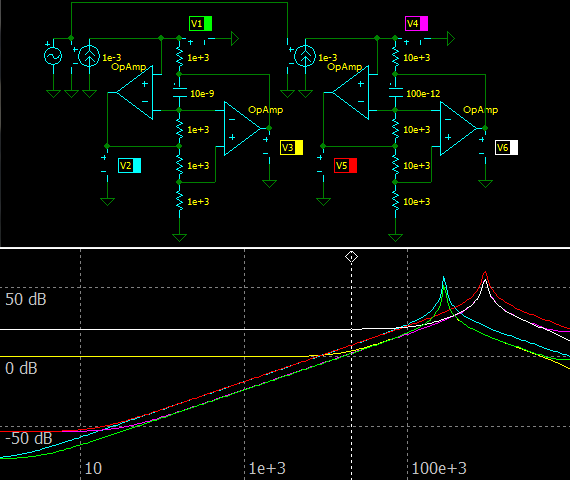
 |
| Gyrator circuits |
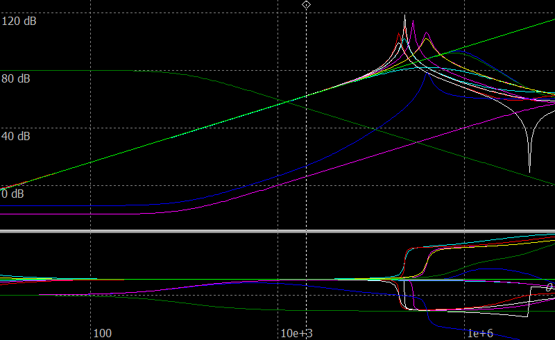 |
| Gyrator circuits, Input impedance |
If a current source is used for frequency sweep, measured voltages are equal to impedances, where 0 dB is 1 Ohm. The marker is set at 20 kHz.
Now let’s arrange the circuits to choose the most interesting ones.
The first parameter is quality factor of inductance at some frequency, which can be evaluated as:
    Im( Z )   2 π F L
Q = ——————— = ———————
    Re( Z )      R
where:
L – the inductance in H;
F – the specified frequency in Hz;
R – the series parasitic resistance in Ohm;
Im( Z ) and Re( Z ) – the image and real parts of the impedance at the frequency;
Q – the quality factor of the inductance at the frequency.
A phase shift from 90° of the ideal inductor at 20 kHz is used instead of calculating the quality factor value. The greater the phase shift, the lower the quality factor.
The second parameter is a peaking frequency; it shows a parasitic capacitance value due to phase shift in the Op Amps which can be evaluated as:
        1
C = ——————————
    L (2 π F)²
where:
L – the inductance in H;
F – the peaking frequency in Hz;
C – the parasitic capacitance in F;
Modified Riordan circuits 1 & 2 give strange responses, so they are dropped.
| Phase shift at 20 kHz | Peaking frequency, Phase above |
|---|---|
|
|
Several circuits have the same peaking frequency, so they are arranged by a peak value assuming that the greater peak, the smaller losses. There is no sharp peak for Antoniou 1, 2, 4.
Pay attention that only some circuits have the phase lower that 90°, like a real inductor. Other gyrators show a phase shift greater than 90°. It means that their equivalent parasitic resistance is negative and oscillations are possible. All such circuits marked in [1] as subject to unstable modes. These circuits also have their phases greater than 90° above their peaking frequencies. Antoniou circuits 1 and 4 are also in this list, but their phases are lower than 90° and Antoniou circuit 4 changes its phase like stable gyrators, so it looks like there is a mistake in [1] and Antoniou circuit 4 is stable. The exception is the Petin gyrator. It shows 90.2° phase shift at 20 kHz but changes phase above its resonance frequency like stable circuits. There is a point around 3 kHz when the Petin gyrator changes its phase shift to values lower than 90°.
See also at the low frequency region. There is a phase shift there too due to limited gain of the Op Amps and it means that Op Amps must have their DC gain as high as possible if a gyrator need to work in the low frequency region.
It is obvious now that only Antoniou circuits 3 & 6 should be used because they are stable and have the lowest losses.
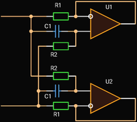
Let’s take a closer look at Antoniou, Riordan and Petin circuits because they look very similar.
Comparison
Renumber Antoniou circuits 3 & 6 as 1 & 2 for convenience.
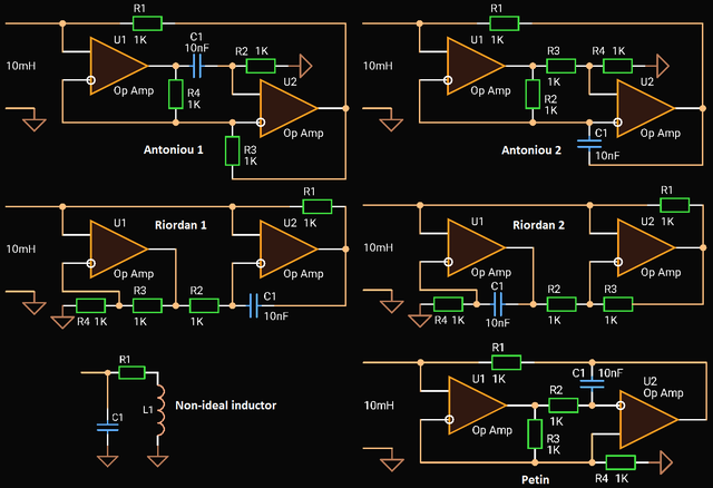 |
| Gyrator circuits to study |
Input Impedances
If we draw circuits and enumerate resistors like in the picture above, assume ideal Op Amps, all the circuits have the same input impedance:
       C1 R1 R2 R4 s
Z(s) = —————————————
            R3
And the inductance is:
    C1 R1 R2 R4
L = ———————————
        R3
It is obvious now that the differences in performance are hidden in parameters of non-ideal Op Amps. The input impedance must be written taking into account the Op Amp limitations.
Antoniou gyrator 1 & 2:
       R1 (R3 + R4) (A + 1) + C1 R1 R2 (A (R4 (A + 1) + R3) + R3 + R4) s
Z(s) = —————————————————————————————————————————————————————————————————
             A² R3 + (R3 + R4) (A + 1) + C1 R2 (R3 + R4) (A + 1) s
Petin gyrator:
                (R4 (A + 1) + R3) (R1 + C1 R1 R2 (A + 1) s)
Z(s) = ——————————————————————————————————————————————————————————————
       R3 (A² + 1) + R4 (A + 1) + C1 R2 [R4 (2 A + 1) + R3 (A + 1)] s
where A is the open-loop gain of both Op Amps, A1=A2=A.
Riordan gyrator 1:
       R1 (R4 (A1 + 1) + R3) + C1 R1 R2 (R4 (A1 A2 + A1 + A2 + 1) + R3 (A2 + 1)) s
Z(s) = ———————————————————————————————————————————————————————————————————————————
          A2 R3 (A1 − 1) + R4 (A1 − A2) + R3 + R4 + C1 R2 (R4 (A1 + 1) + R3) s
Riordan gyrator 2:
       R1 (R1 (A2 + 1) + R3) + C1 R1 R4 (R2 (A1 A2 + A1 + A2 + 1) + R3 (A1 + 1)) s
Z(s) = ———————————————————————————————————————————————————————————————————————————
          R3 (A2 (A1 − 1) + 1) + R2 + C1 R4 (R3 (A1 − A2 + 1) + R2 (A1 + 1)) s
There is (A1−A2) member in Riordan gyrators, so the difference in Op Amp gains affects the circuit performance. It also means that their behavior can change with component values, and instabilities are possible.
Widely used Op Amps are compensated and their open-loop gain is the function of frequency:
        GBW
A(s) = —————
       2 π s
where:
A(s) – the Op Amp open-loop gain, unlimited maximum gain is assumed;
GBW – the Op Amp Gain-Bandwidth product, the unity gain radial frequency in rad/s;
s – the complex frequency;
Therefore gyrator input impedances are complex third order functions.
Quality factor
Unfortunately, equations for quality factors are more complex.
The quality factor for Antoniou circuits 1 & 2 is:
                   GBW² (GBW C1 R2 R4 + R3 + R4)(GBW R3 − ω² C1 R2 (R3 + R4))
Q = ——————————————————————————————————————————————————————————————————————————————————————————————
    ω (R3 + R4)(ω² (C1² R2² [(R3 + R4) ω² + R3 GBW²] + R3 + R4) + GBW² [GBW C1 R2 (R4 − R3) + R4])
Assume R1=R2=R3=R4, then:
       GBW² (GBW C1 R + 2)(GBW − 2 ω² C1 R)
Q = ——————————————————————————————————————————
    2 ω (ω² [C1² R² (2 ω² + GBW²) + 2] + GBW²)
At low frequencies, when 1000×ω < GBW:
Q ≈ 300 GBW / ω
For Petin and both Riordan circuits the equations are too long, so assume R1=R2=R3=R4.
For both Riordan circuits:
     GBW (C1 R GBW³ + GBW² - ω² (C1 R [C1 R (4 ω² + GBW²) + 8 GBW] + 4))
Q = ——————————————————————————————————————————————————————————————————————
    ω (ω² (C1 R [C1 R (4 ω² + GBW²) + 8 GBW] + 4) - GBW² (4 GBW C1 R + 3))

Q ≈ −GBW / (4 ω)
For Petin circuit:
               GBW² (C1 R (GBW² - ω² (3 C1 GBW R + 4)) + GBW)
Q = ————————————————————————————————————————————————————————————————————————
    ω (ω² (C1 R [C1 R (4 w² + 7 GBW²) + 8 GBW] + 4) - GBW² [2 C1 GBW R + 1])

Q ≈ −GBW / (2 ω)
GBW here in rad/s. The larger GBW the better.
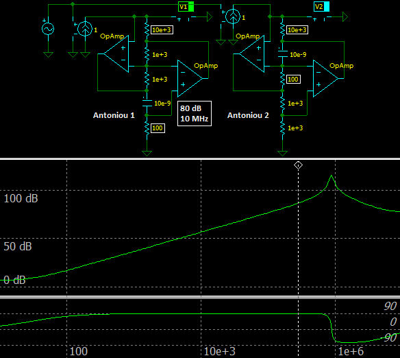
The equations show that the only Antoniou circuits have positive parasitic resistance like real inductors. It is negative in other circuits. They also match with the results of simulation, because Antoniou circuits show the best GBW utilization (89.98° @ 20 kHz), and Petin circuit (90.2° @ 20 kHz) do it better than Riordan circuits (90.45° @ 20 kHz).
There is the (R4−R3) member in the equation for Antoniou circuits, so resistor tolerances affect the quality factor value and it looks like that is possible to change the sign of the equivalent parasitic resistance. Equations for Riordan and Petin circuits do not show such explicit dependencies.
Calculated values are:
Antoniou 1 & 2: Q = 60790 (89.98° @ 20 kHz);
Petin: Q = −250.5 (90.2° @ 20 kHz);
Riordan 1 & 2: Q = −124.8 (90.45° @ 20 kHz);
Now we can narrow our list down to Antoniou circuits only.
Parasitic parameters
The peaking frequency and the parasitic capacitance for Antoniou gyrators are:
            √{ GBW R3 }
Fp = ————————————————————————
     √{ 2 π C1 R2 (R3 + R4) }

        R3 + R4
Cp = —————————————
     2 π GBW R1 R4
GBW here in Hz. The equations show that the GBW should be as large as possible to keep the parasitic capacitance low. They also show that if R1=R2=R3=R4, the resistance values can be increased to make the parasitic capacitance lower.
Let’s verify the equations. R1=R2=R3=R4=1 kOhm, C1=10 nF and Op Amps with GBW of 10 MHz were used in the simulation.
                  √{ 10 MHz × 1 kOhm }
Fp = ———————————————————————————————————————————— ≈ 282 kHz
     √{ 2π × 10 nF × 1 kOhm × (1 kOhm + 1 kOhm) }

            1 kOhm + 1 kOhm
Cp = ————————————————————————————— ≈ 32 pF
     2π × 10 MHz × 1 kOhm × 1 kOhm
The values correspond perfectly to the values in the simulation!
Peak reducing
There is a recommendation in [4]:
The peaking can be eliminated by adding a resistor in series with the gyrator’s capacitor, roughly equal to its reactance at the peaking frequency.
Compute the capacitor reactance for our case:
        1                 1
Zc = ———————— = ———————————————————— ≈ 56 Ohm
     2 π F C1   2 π × 282 kHz ×10 nF
 |
| Peak reduction |
The simulation confirms it, but unfortunately the quality factor suffers too.
Resistor values
The equations for quality factors show that R3 and R4 resistor values affect the quality factor value. Change them by 5%.
 |
| Resistor tolerances affect stability |
Now there is 90° crossover point at about 20 kHz in Antoniou 1 & 2 circuits, where their equivalent resistance changes its sign. Thus, R3 and R4 resistor tolerances affect the circuit performance and stability, their values must be equal.
Recall other equations and since R3=R4, they can be simplified:
    C1 R1 R2 R4
L = ——————————— = C1 R1 R2
        R3

        R3 + R4          1
Cp = ————————————— = ——————————
     2 π GBW R1 R4   2 π GBW R1
The equations show that the parasitic capacitance can be reduced by increasing the R1 value.
Let’s verify it and increase the R1 value. The R2 value is recalculated to keep the inductance unchanged.
 |
| Resistors affect a peaking frequency |
The marker shows the initial peaking frequency, ~282 kHz. The simulation confirms that a parasitic capacitance can be reduced by increasing an R1 value. But unfortunately it also increases losses.
Op Amp Bandwidth
We have seen that Op Amp’s GBW is important. The GBW affects the quality factor and peaking frequency.
The first estimation is to set
The second estimation is to set some factor and calculate the GBW to get the peaking frequency Fp greater than the maximum working frequency,
Set
The second estimation for Antoniou circuits at R1=R2=R3=R4=R:
GBW ≥ C1 R 4π (4 Fmax)² = 10 nF × 1 kOhm × 4π × (4 × 20 kHz)² = 800 kHz
Therefore for the audio frequency range Op Amps with GBW of 4 MHz at least should be used.
Working voltage range
It is obvious that working voltage must not be greater than Op Amp’s input common voltage range, but what is the Op Amp output voltage?
Let’s set 1 mA working current and look at the Op Amp output voltages at different component values but the same simulated inductance.
 |
| Voltage swings at 1 mA |
The output voltage swing below 20 kHz is about 0 dB (1 V) for the first circuit and about +20 dB (10 V) for the second circuit! And it is more than +60 dB (1 kV) at the peaking frequency!
Thus it is obvious now that real gyrators are able to work only at low currents and low frequencies with reasonable component values.
The charts also confirm that peaking frequencies can be increased by making resistor values large. So, though low resistor values are preferable to keep their thermal noise lower, at low currents their values can be increased to decrease the parasitic capacitance.
Berndt & Dutta Roy’s Gyrator
 |
| Berndt & Dutta Roy’s Gyrator, RL gyrator |
This gyrator is described in [5] and it works like a series RL network.
Design Equations
For the ideal Op Amp the impedance between the input and the ground wire is:
       R1 + C1 R1 R2 s
Z(s) = ———————————————
         1 + C1 R1 s
And at low frequencies it is close to the impedance of the RL network:
Z(s) = R + L s
R = R1, L = C1 R1 R2
R1 is the Op Amp load resistance, so the Op Amp must be able to drive such a load.
The equations predict that the RL gyrator behavior at large R1 values can be far from expected, because the R1 value is in the denominator too.
Let’s compute somehow component values for 2 cases: 10 Ohm and 10 mH, 1 kOhm and 10 mH. Then use the values in a simulator with ideal and non-ideal Op Amps.
 |
| RL gyrator, 10 Ohm 10 mH |
 |
| RL gyrator, 1 kOhm 10 mH |
The simulations show that RL gyrator’s behavior is far from the RL network when the resistance is 1 kOhm even with the ideal Op Amp, as predicted with the equations above. But the equations also show a way to get the desired behavior: the C1 value must be reduced to compensate the large R1 value.
 |
| RL gyrator, 1 kOhm 10 mH, corrected |
The markers in all pictures above show the frequencies where phases and quality factors meet their maximums.
We can use the phase peaking to determine a maximum working frequency and compute component values more accurately. Assuming the ideal Op Amp and R1 << R2, the phase peaking frequency is:
             1
Fph ≈ ————————————————
      2π C1 √{ R1 R2 }
And the maximum quality factor is:
         R2 − R1
Qph ≈ ————————————
      2 √{ R1 R2 }
If an Op Amp has a limited GBW, a phase peaking frequency is slightly lower and there is peaking in magnitude too. This peak can be treated as a parasitic capacitance added in parallel with the RL network.
For a non-ideal Op Amp the input impedance of the circuit is:
           R1 + (C1 R1 R2) s
Z(s) = ——————————————————————————
       1 + C1 [R1 + R2/(A + 1)] s
where A is the Op Amp’s transfer function.
The quality factor now is (GBW in rad/s):
             C1 ω [GBW² (R2 − R1) − ω² (GBW C1 R2² + R1)]
Q = —————————————————————————————————————————————————————————————
    ω² (C1 R2 [C1 ω² (R1 + R2) + GBW (GBW C1 R1 − 1)] + 1) + GBW²
Assuming that R1 << R2:
                    1
Q ≈ —————————————————————————————————
    C1 R2 ω³ / (GBW²) + 1 / (C1 R2 ω)
The peaking frequency and parasitic capacitance are (GBW here in Hz):
       √{ GBW }
Fp ≈ —————————————
     √{ 2π C1 R2 }

         1
Cp ≈ ——————————
     2 π GBW R1
The last simulation shows that the peaking frequency is ~400 kHz, and the equation gives:
        √{ GBW }            √{ 10 MHz }
Fp ≈ ————————————— = —————————————————————————— ≈ 400.5 kHz
     √{ 2π C1 R2 }   √{ 2π × 62 pF × 160 kOhm }
Now a minimum required GBW must be found. The simplest way is just use some factor and define
Example
Let’s compute an RL gyrator with 1000 Ohm resistance and 10 mH inductance working up to 20 kHz.
Quality factor of the network at 20 kHz is:
    10 mH × 2π × 20 kHz
Q = ——————————————————— ≈ 1.26
          1 kOhm

R1 = 1 kOhm (E96)
Find the minimum R2 value and the maximum C1 value:
R2 = R1 (2 Q [Q + √{ Q² + 1 }] + 1) = 1 kOhm × (2 × 1.26 × (1.26 + √{ 1.26² + 1 }) + 1) ≈ 8.25 kOhm (E96)

       L           10 mH
C1 = ————— = —————————————————— ≈ 1.2 nF (E24)
     R1 R2   1 kOhm × 8.25 kOhm
Now we need to find a minimum GBW.
The first approximation:
GBW ≥ 100 F ≈ 100 × 20 kHz ≈ 2 MHz
The second approximation:
GBW ≥ 2π C1 R2 (2 F)² = 2π × 1.2 nF × 8.25 kOhm × (4 × 20 kHz)² ≈ 400 kHz
So, the maximum value, 2 MHz, will be used.
Use a simulator to verify our solution.
 |
| RL gyrator, 1 kOhm 10 mH, example |
Berndt & Dutta Roy’s Floating RL Gyrator
 |
| Floating RL Gyrator |
Design Equations
They are similar to the RL gyrator described above. The impedance between two ports for the ideal Op Amp and high load impedances is:
       R1 + C1 R1 R2 s
Z(s) = ———————————————
        1 + 2 C1 R1 s
And at low frequencies it is close to the impedance of the RL network:
Z(s) = R + L s
R = R1, L= C1 R1 R2
Assuming the ideal Op Amp, R1 << R2 and high load impedances, the phase peaking frequency is:
              1
Fph ≈ ——————————————————
      2π C1 √{ 2 R1 R2 }
And the maximum quality factor is:
         R2 − 2 R1
Qph ≈ ——————————————
      2 √{ 2 R1 R2 }
For a non-ideal Op Amp the impedance between two ports is:
                 (A + 1)(R1 + C1 R1 R2 s)
Z(s) = ————————————————————————————————————————————
       (2 A + 1) / 2 + s C1 (R2 / 2 + 2 R1 (A + 1))
where A is the Op Amp’s transfer function.
Assuming R1 << R2, the peaking frequency and parasitic capacitance are:
       √{ GBW }
Fp ≈ ————————————
     √{ π C1 R2 }

         1
Cp ≈ ——————————
     4 π GBW R1
A minimum required GBW can be found using the same relations as for RL gyrator. GBW ≥ k Fmax, Fmax is the maximum working frequency and k ≥ 100.
Example
Let’s compute a floating RL gyrator with 1000 Ohm resistance and 10 mH inductance working up to 20 kHz.
Quality factor of the network at 20 kHz is:
    10 mH × 2π × 20 kHz
Q = ——————————————————— ≈ 1.26
          1 kOhm

R1 = 1 kOhm (E96)
Find a minimum R2 value and a maximum C1 value:
R2 = 2 R1 (2 Q [Q + √{ Q² + 1 }] + 1) = 2 × 1 kOhm × (2 × 1.26 × (1.26 + √{ 1.26² + 1 }) + 1) ≈ 16.5 kOhm (E96)

       L           10 mH
C1 = ————— = —————————————————— ≈ 620 pF (E24)
     R1 R2   1 kOhm × 16.5 kOhm
Now we need to find a minimum GBW.
The first approximation:
GBW ≥ 100 F ≈ 100 × 20 kHz ≈ 2 MHz
The second approximation:
GBW ≥ π C1 R2 (2 F)² = π × 1.2 nF × 8.25 kOhm × (4 × 20 kHz)² ≈ 200 kHz
So, the maximum value, 2 MHz, will be used.
Use a simulator to verify our solution.
 |
| Floating RL gyrator, 1 kOhm 10 mH, example |
The simplest simulated inductor
 |
| Transimpedance amplifier simulates an inductance |
It is a transimpedance amplifier, of course! And ~88.8° at 20 kHz is not so bad. Parasitic capacitances are added to the right circuit to do it more realistic, the phase is ~74.2° there.
Input impedance of the transimpedance amplifier is:
         R
Z(s) = —————
       A + 1
Since gain of a compensated Op Amp is frequency dependent:
       GBW
A(s) = ———
        s

         R s
Z(s) = ———————
       GBW + s
GBW here in rad/s. At low frequencies when ω << GBW:
        R
Z(s) ≈ ——— s
       GBW
And the inductance is:
     R
L ≈ ———
    GBW
For the example in the picture, where GBW is 1 MHz:
R ≈ GBW L ≈ 2π × 1 MHz × 0.159 H ≈ 1 MOhm
GBW of an Op Amp is not a constant. For example, it can vary with supply voltages, so accuracy is not very good.
Let’s have fun with the gyrators
Gyrators are usually used in active filters to replace inductors. But can they be used in switching-mode power supplies?
So, we want to build a split-rail DC/DC converter.
Input: +12 VDC, Output: +5 VDC 1 A, −5 VDC 1 A.
Let’s use well-known topologies: “Buck” to get +5 V and “Inverting Buck-Boost” to get −5 V. Using well-known equations, find component values for both topologies.
Buck:
Inverting Buck-Boost:
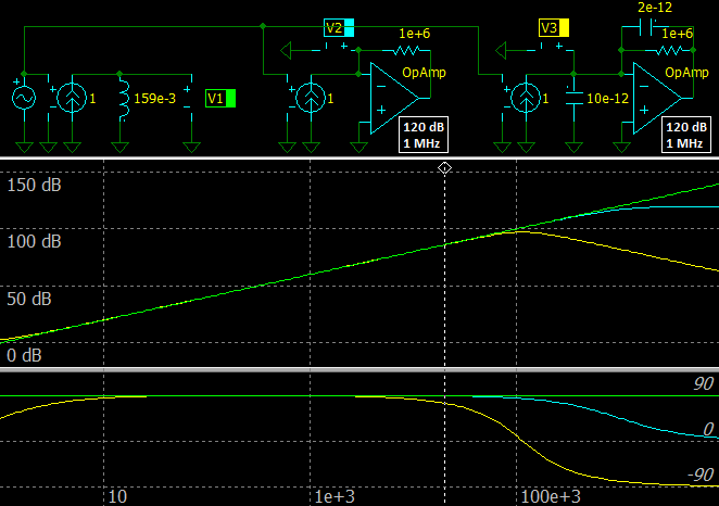
Since the switching frequency is 50 kHz and there are harmonics, Op Amps with 2 A output, GBW of 100 MHz, a maximum gain of 60 dB are used powered from extra +12 V and −12 V rails. Energy cannot appear from nowhere, isn’t it? Losses should be low, 50 mOhm is a good value for the equivalent series resistance. Compute resistor and capacitor values, draw circuits, enter values and run a simulator!
 |
| Split-Rail DC/DC converter with gyrators |
Voila! It works! Used component values are far from optimal, in fact they are inductances up to about 60 kHz only, but still it works! In the simulator, of course.
Conclusion
Gyrators can be used to replace inductances in electronics circuits. The advantages are large inductance values and predictability of parameters. The disadvantage is a limited frequency range.
- Only Antoniou 3 & 6 circuits [1] should be used. Equations for both circuits are equal. Resistors with equal values and 1% tolerances or better are preferable.
- Phase shift introduced by limited Op Amp’s GBW looks like a parasitic capacitance and sum with an Op Amp input capacitance causing resonance peaking.
- A peaking frequency can be changed by using different resistor values, but it reduces a quality factor value, so the best choice is to use equal resistor values at all positions.
- Resonance peak magnitude can be reduced by adding a resistor in series with the capacitor, but it reduces a quality factor value.
- Berndt & Dutta Roy’s topology is the simplest and suitable when an RL network needs to be replaced.
- Op Amps in gyrators must have their DC gain and GBW as large as possible. For the audio frequency range of
20 Hz … 20 kHz :gain > 100 dB andGBW > 4 MHz are preferable.
References
- James John Kulesz, «A study of gyrator circuits».
- BBC, R.H.M. Poole, “The Taming of the Gyrator”.
- Radio 1996 №11, p.33.
- P. Horowitz, W. Hill, “The Art of Electronics, 3-d Edition”.
- D.F. Berndt, S.C.D. Roy, “Inductor simulation using a single unity gain amplifier”.
- Burr-Brown, “A low noise, low distortion design for antialiasing and anti-imaging filters”.
- TI, “An audio circuit collection, Part 3”.
- Manjula V. Katageri, “LC Active Low Pass Ladder Filter by Lossless Floating Inductor Gyrator”.
- «idealCircuit», a simulator.
- «Circuit Calculator», an electronics circuit design tool for Android.
