An operational amplifier has the internal compensation circuit for stability which limits its working bandwidth. Frequency response of the compensated Op Amp has slope of −6 dB/octave or −20 dB/decade. Unity gain frequency defines the bandwidth where the Op Amp is able to amplify a signal. If we multiply the gain and frequency at any point, the result is the same, allowing us to use this parameter to select the appropriate Op Amp. It is called Gain-Bandwidth Product, GBW or GBP. The limited open-loop gain introduces a closed-loop gain and phase error.
But we want to optimize our circuits, right?
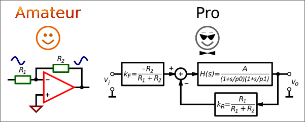
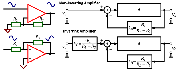 |
| Closed-loop gain of the Non-Inverting and Inverting Amplifier |
The closed-loop gain of the non-inverting amplifier is:
       A
G = ———————
    1 + A β
and for the inverting amplifier:
      A (1 − β)
G = − —————————
       1 + A β
where:
A is the open-loop gain;
β is the feedback fraction.
Let’s calculate, for example, an inverting amplifier with desired gain of 1 when
     A (1 − β)     100 × (1 − 0.5)     50
G= − ————————— = − ——————————————— = − —— ≈ −0.98
      1 + A β       1 + 100 × 0.5      51
and A=1:
     A (1 − β)     1 × (1 − 0.5)
G= − ————————— = − ————————————— ≈ −0.333
      1 + A β       1 + 1 × 0.5
But to make a real Op Amp stable, A is frequency dependent and there is a phase shift, how you can see in the picture below.
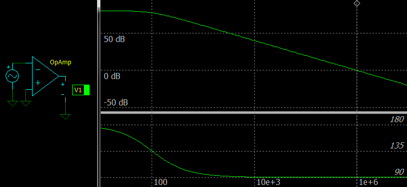 |
| Frequency response of the compensated Op Amp without a feedback network |
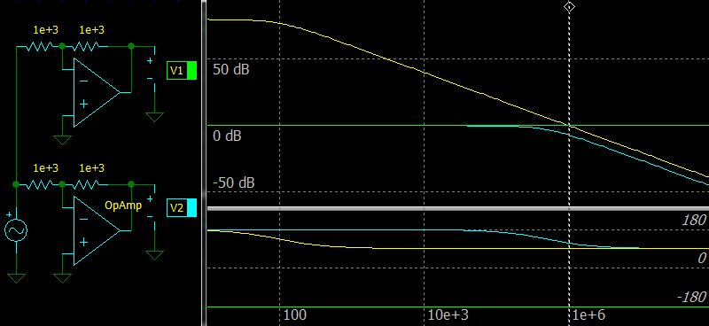 |
| The inverting amplifier with ideal and compensated Op Amp. |
The figure shows the difference between the ideal and compensated Op Amp with GBW = 1 MHz. You can see that the cyan line of the compensated Op Amp is always below the yellow line showing its open-loop gain and there must be some margin.
However, the simulator shows that gain at 1 МГц is not -9.55 dB, but about -7 dB due to a phase shift at the output.
The closed-loop gain error versus gain margin for the non-inverting amplifier looks likes that:
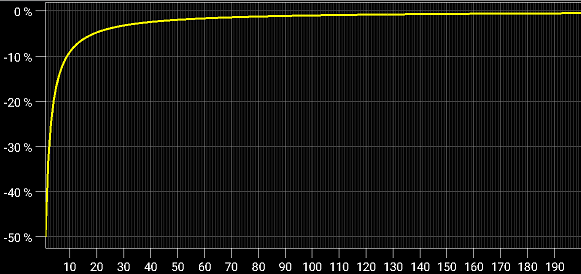 |
| Closed-loop gain error vs Gain margin of the non-inverting amplifier. |
Error compensation for 2-nd order low-pass filter
This equation is usually used to compute the GBW of an Op Amp:
GBW(Hz) = 100 × Q × G × F3
where:
Q is the quality factor of the filter;
G is the specified gain;
F3 is the cutoff frequency at -3 dB;
100 is the gain margin.
Why? A low-pass filter with
              Q
β = ————————————————————— ≈ Q
    sqrt(1 − 1 / (4 Q^2))
The most of used filters are low-pass filters for ADCs and DACs. So even for an LPF with 150 kHz an Op Amp with GBW of 15 MHz is desirable.
Texas Instruments’ engineers shared a method to reduce the requirement in [1][2].
Let’s try to figure out how to use their equations in practice.
Multiple FeedBack LPF
Let’s compute a 2-nd order LPF with bandwidth of 150 kHz, gain of 1 and quality factor of 0.707.
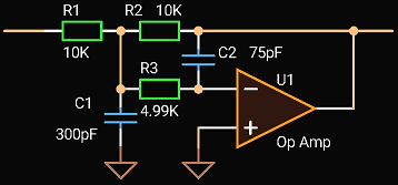 |
| 2-nd order MFB LPF |
The required GBW is:
GBW(Hz) = 100 × Q × G × F3 = 100 × 0.707 × 1 × 150 kHz ≈ 10.5 MHz
Let’s try to use an Op Amp with GBW of 1 MHz.
Add R4 in series with C2:
            1                   1
R4 = ———————————————— = ——————————————————— = 2122 ≈ 2.1k (E96)
     2 × π × GBW × C2   2 × π × 1MHz × 75pF
Change R3:
R3' = R3 − R4 = 4990 − 2100 = 2868 ≈ 2.87k (E96)
And finally enter the values into a simulator:
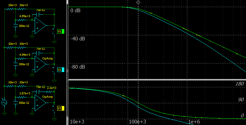 |
| Error compensation for 2-nd order MFB LPF |
The top circuit and green color on the charts: the ideal amplifier.
The middle circuit and cyan color on the charts: the Op Amp with GBW of 1 MHz.
The bottom circuit and yellow color on the charts: the Op Amp with GBW of 1 MHz and with the error compensation.
When R3 is too low, the R3’ value may be negative. In such cases you should recalculate the filter with a greater R3 value.
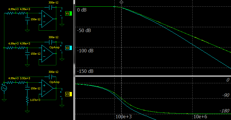
Sallen-Key LPF
Let’s compute a 2-nd order LPF with bandwidth of 150 kHz, gain of 1 and quality factor of 0.707.
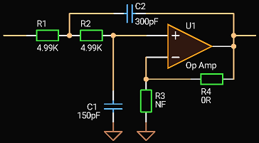 |
| 2-nd order Sallen-Key LPF |
The required GBW is:
GBW(Hz) = 100 × Q × G × F3 = 100 × 0.707 × 1 × 150kHz ≈ 10.5 MHz
Let’s try to use an Op Amp with GBW of 1 MHz.
Add R5 in series with C1:
            R3 + R4                  ∞ + 0                      1
R5 = ————————————————————— = ———————————————————————— = ———————————————————— = 1061 ≈ 1.07k (E96)
     2 × π × GBW × C1 × R3   2 × π × 1MHz × 150pF × ∞   2 × π × 1MHz × 150pF
Change R2:
R2' = R2 − R5 = 4990 − 1070 = 3920 = 3.92k (E96)
And finally enter the values into a simulator:
 |
| Error compensation for 2-nd order Sallen-Key LPF |
The top circuit and green color on the charts: the ideal amplifier.
The middle circuit and cyan color on the charts: the Op Amp with GBW of 1 MHz.
The bottom circuit and yellow color on the charts: the Op Amp with GBW of 1 MHz and with the error compensation.
Error compensation for Type II compensation network with Op Amp
Let’s try to apply the same method to the Type II compensation network with Op Amp used in switching-mode power supplies.
Consider a Type II circuit with parameters: the zero at 2 kHz, the pole at 300 kHz, the middle gain is 0 dB.
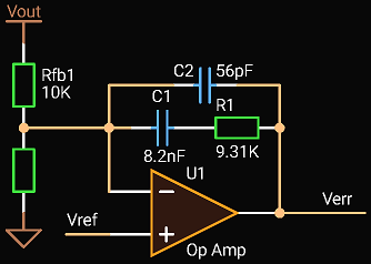 |
| Type 2 compensation with Op Amp |
Conservative calculation of the required GBW:
GBW(Hz) = M × Fpole × Gfp = 100 × 300kHz × 0.707 ≈ 21 MHz
where:
M=100 is the gain margin of the Op Amp at a frequency in times;
Fpole is the pole frequency in Hz;
Gfp is the gain at the pole frequency in times.
Christophe Basso in [4] gives another calculation:
GBW(Hz) = M × (20 Fcross) × Gfc = 20 × 20 × 5kHz × 1 ≈ 2 MHz
where:
M=20 is the gain margin of the Op Amp at a frequency in times;
20 Fcross is the frequency with maximum phase boost in Hz with the factor to account the pole position;
Gfc is the gain at the Fcross frequency in times.
The transfer function of the circuit is:
                         (C1 R1 s + 1)
H(s) = − ——————————————————————————————————————————————
         (s Rfb1 (C1 + C2))(s C1 C2 R1 / (C1 + C2) + 1)
Add R2 in series with C2. The new transfer function is:
                      (1 + C1 R1 s) (1 + C2 R2 s)
H(s) = − ——————————————————————————————————————————————————————
         (s Rfb1 (C1 + C2)) (s C2 C1 (R2 + R1) / (C1 + C2) + 1)
Change the C2 value and find the R2 value:
                  1
C2' = C2 − ————————————————
           2 × π × GBW × R1
            1
R2 = —————————————————
     2 × π × GBW × C2'
Now try to use an Op Amp with
Recalculate the circuit values using the equations above and see the result.
Adjust the C2 value:
                     1
C2' = 56pF − —————————————————— = 40pF ≈ 39pF (E24)
             2 × π × 1MHz × 10k
The R2 value:
             1
R2 = ——————————————————— = 4k ≈ 3.9k (E24)
     2 × π × 1MHz × 39pF
And finally enter the values into a simulator:
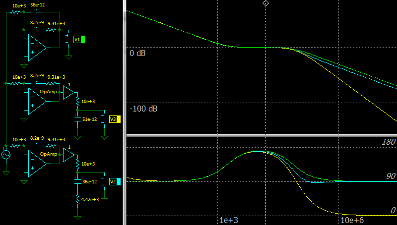
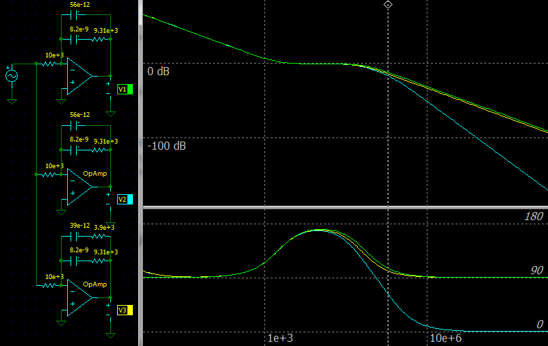 |
| Error compensation for Type 2 compensation network with Op Amp |
The top circuit and green color on the charts: the ideal amplifier.
The middle circuit and cyan color on the charts: the Op Amp with GBW of 1 MHz.
The bottom circuit and yellow color on the charts: the Op Amp with GBW of 1 MHz and with the error compensation.
Error compensation for Type II compensation network with Optocoupler without Fast Lane
There are 2 variants of the circuit: with an Op Amp and a shunt regulator like TL431.
We will use the same parameters: the zero at 2 kHz, the pole at 300 kHz, the middle gain is 0 dB, the current transfer ratio of an optocoupler is 1.
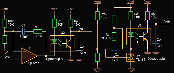 |
| Type 2 compensation with Optocoupler without Fast Lane |
The transfer function of both circuits is (C1=Cz, R1=Rz):
         CTR Rp       (1 + C1 R1) s
H(s) = − —————— —————————————————————————
           Rd   (C1 Rfb1 s) (1 + Cp Rp s)
where CTR is the current transfer ratio of the optocoupler.
Add Rc in series with Cp. The new transfer function is:
         CTR Rp   (1 + C1 R1 s) (1 + Cp CRc s)
H(s) = − —————— ————————————————————————————————
           Rd   (C1 Rfb1 s) (1 + Cp (Rp + Rc) s)
Change the C2 value and find the Rc value:
                  1
Cp' = Cp − ————————————————
           2 × π × GBW × Rp
            1
Rc = —————————————————
     2 × π × GBW × Cp'
Try to use an Op Amp with
Recalculate the circuit values using the equations above and see the result.
Adjust the Cp value:
                     1
Cp' = 51pF − —————————————————— = 35.1pF ≈ 36pF (E24)
             2 × π × 1MHz × 10k
The Rc value:
             1
Rc = ——————————————————— = 4.421k ≈ 4.42k (E96)
     2 × π × 1MHz × 36pF
The extra DC gain is:
    CTR Rp   1 × 10k
A = —————— = ——————— = 1
      Rd       10k
And finally enter the values into a simulator:
 |
| Error compensation for Type 2 compensation network with Optocoupler without Fast Lane |
The top circuit and green color on the charts: the ideal amplifier.
The middle circuit and yellow color on the charts: the Op Amp with GBW of 1 MHz.
The bottom circuit and cyan color on the charts: the Op Amp with GBW of 1 MHz and with the error compensation.
Do not forget that a real optocoupler has a parasitic capacitance and its value should be taken into account.
Conclusion
The described methods help to reduce the requirement to the Gain-Bandwidth of a used Op Amp and cost of circuits.
For filters, they work well with commonly used quality factors below 1.
References
- TI, Vito Shen, Thomas Kuehl, «Compensation Methodology for Error in Multiple-Feedback Low-Pass Filter, Caused by Limited Gain-Bandwidth of Operational Amplifiers»
- TI, Vito Shen, Thomas Kuehl, «Compensation Methodology for Error in Sallen-Key Low-Pass Filter, Caused by Limited Gain-Bandwidth of Operational Amplifiers»
- Christophe Basso, «Understanding Op Amp Dynamic Response In A Type-2 Compensator (Part 1): The Open-Loop Gain»
- Christophe Basso, «Understanding Op Amp Dynamic Response In A Type-2 Compensator (Part 2): The Two Poles»
- Christophe Basso, “The TL431 in Switch-Mode Power Supplies loops”
- «idealCircuit», simulator, Windows
- «Circuit Calculator», an electronics design tool for Android
