Comments 10
micdrop.jpg
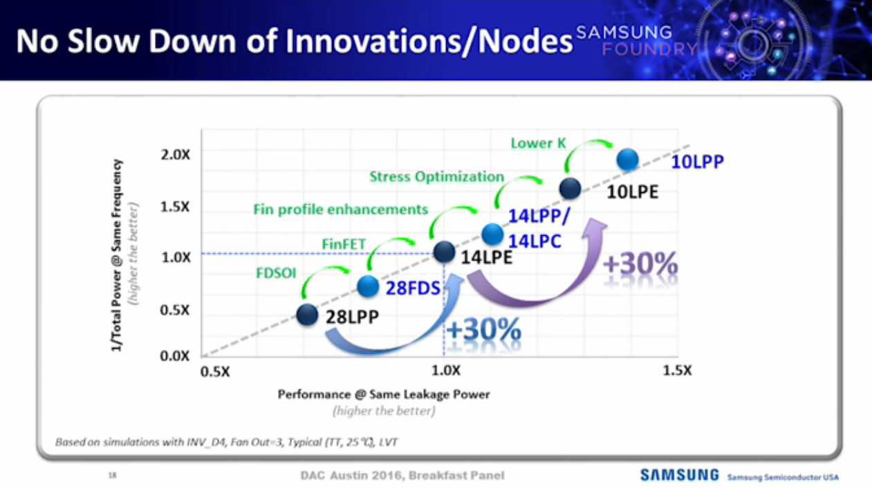
Как можно писать новость по заметке Reuters с 3 абзацами? Есть же нормальный пресс-релиз, в котором присутствуют термины FinFET и названия: 10LPE (начало 2017), 10LPP (конец 2017):
https://news.samsung.com/global/samsung-starts-industrys-first-mass-production-of-system-on-chip-with-10-nanometer-finfet-technology
Samsung’s new 10nm FinFET process (10LPE) adopts an advanced 3D transistor structure with additional enhancements in both process technology and design enablement compared to its 14nm predecessor, allowing up to 30-percent increase in area efficiency with 27-percent higher performance or 40-percent lower power consumption. In order to overcome scaling limitations, cutting edge techniques such as triple-patterning to allow bi-directional routing are also used to retain design and routing flexibility from prior nodes.
Following the introduction of Samsung’s first-generation 10nm process (10LPE), its second generation process (10LPP) with performance boost is targeted for mass production in the second half of 2017. The company plans to continue its leadership with a variety of derivative processes to meet the needs of a wide range of applications.
Production level process design kits (PDK) and IP design kits are currently available for design starts.
SoCs with 10nm process technology will be used in digital devices launching early next year and are expected to become more widely available throughout 2017.
Anand нашел старый слайд с планами Samsung: http://www.anandtech.com/show/10765/samsung-10nm-massproduction — http://images.anandtech.com/doci/10765/dac.png (DAC 2016)
В апреле уже была информация о планах http://www.sammobile.com/2016/04/22/samsung-releases-more-details-about-its-7nm-and-10nm-chip-manufacturing-processes/
10LPE = Low Power Early; 10LPP = Low Power Plus
Они отложили EUV на 7 нм (подробная статья от eetimes — http://www.eetimes.com/document.asp?doc_id=1330632 Samsung to Ship 10nm SoCs in 2016. Korean giant plans 7nm with EUV in late 2018)
и им пришлось использовать triple patterning для критических слоёв. Пример того, как может выглядеть triple patterning "LELELE" — http://spie.org/newsroom/4539-triple-patterning-in-10nm-node-metal-lithography (2012, Synopsys).
На практике это значит кратное удорожание mask set и необходимость еще больших тиражей каждого продукта для окупаемости производства (= меньше разных продуктов), а также длительное производство чипа — ~3-3.5 месяца (по подсчетам http://semiengineering.com/finfet-rollout-slower-than-expected/ 2015 года — 1.3 дня на литографию, ~50 литографий на 28 нм 11М, 66 на 16/14 нм, а тут в 1,5 раза больше критических масок из-за TP LELELE). Сильно растет сложность проектирования: http://semiengineering.com/finfet-rollout-slower-than-expected/ — FinFET проекты "средней СнК" на 16/14 нм были в 3 раза дороже планарных 20 нм — 80 и 30 млн $ по данным Gartner без учета стоимости масок и производства; для 14 нм — ~200 человеко-лет трудозатрат + 9-12 месяцев производства. PDK стал широко доступен только сейчас, проектирование стало еще сложнее, чем для 14 нм (а уже там из-за вариаций техпроцесса вместо классических 4 углов TT FF SS FS SF, с 2005 года применялись ограничено, было уже около 20 — "four corners is now more like 20 corner"), а производство — еще дольше...
Также eetimes сообщает, что Samsung не раскрыл точных размеров элементов. Там же — о заявлениях других производителей про "10нм", прогнозы рынка, оценки стоимости производства пластины и потенциальные клиенты http://www.eetimes.com/document.asp?doc_id=1330632 & http://www.eetimes.com/document.asp?doc_id=1330632&page_number=2
Hong also declined to provide any specific metrics, such as minimum gate pitch, of the 10nm process. Process and IP design kits for the 10nm node are available now, Samsung said. The company described a 10nm SRAM cell at a technical conference in January.
Samsung is the last of the big foundries to give details on its plans at 10nm. TSMC and Intel announced — in September and in August respectively — they are ramping 10nm processes that will be in production next year. Globalfoundries announced in September will skip the 10nm node which it said does not push triple-patterning lithography to its limits, driving to a 7nm process it aims to have in production in late 2018.
Intel said its 10nm process will have sport a 54nm gate pitch, packing transistors more densely than any competitors—a claim most analysts accept. Foundries use of names such as 10nm no longer points to any specific metric, so mileage is expected to vary considerably between companies.
TSMC suggested its 10nm node will be fairly short lived compared to its 7nm process which could have limited availability in 2017.
International Business Strategies (IBS) estimates ...10/7 nm wafers will be sold in 2025 with an average wafer price of $8,000 creating a $17.6 billion market up from first year sales of 322,000 wafers in 2017. Key customers will include processor vendors AMD, Apple, Huawei’s HiSilicon, MediaTek, NVidia, Qualcomm and Xilinx as well as internal consumption in Samsung.
Платная статья о тестовых SRAM чипах на 10 нм (апрель 2016): Song, Taejoong, et al. "17.1 A 10nm FinFET 128Mb SRAM with assist adjustment system for power, performance, and area optimization." 2016 IEEE International Solid-State Circuits Conference (ISSCC). IEEE, 2016. — http://ieeexplore.ieee.org/xpls/abs_all.jsp?arnumber=7418029; новости по мотивам: http://www.eetimes.com/document.asp?doc_id=1328866 https://www.semiwiki.com/forum/content/5620-10nm-sram-projections-who-will-lead.html
Related: TSMC started working on 7nm production earlier this year.
If AMD’s next-gen processors are coming from GlobalFoundries, that means they’re probably going to be on the 7-nanometer node, not the 10nm node which Intel will be using – Intel has heavily invested in the 10nm node, so it’s unlikely they’d skip it entirely.
What does all this mean for your PC? Well, it means that in a few years AMD might have have a slight edge over Intel, with processors that could do a lot more with a lot less. A chip built on the 10nm node could be at a serious disadvantage against a similar processor built on a 7nm node.
Naturally, AMD’s upcoming processor, the Zen+, is more than likely going to remain a 14nm chip. This revamped agreement with GlobalFoundries won’t bear fruit for a while, but it’s definitely an interesting move that could very well change the game for AMD and Intel.
Read more: http://www.digitaltrends.com/computing/amd-skipping-10nm-for-7nm/#ixzz4NPwgxWOs
Samsung заявила о старте массового производства чипов с архитектурой 10 нм