Welcome to RISC-V era!
Solutions based on the open standard instruction set architecture RISC-V are currently increasing their presence on the market. Microcontrollers from Chinese colleagues are already in serial production; Microchip is offering interesting solutions with FPGA on board. The ecosystem of software and design tools for this architecture are also growing. Seeming previously unshaken leaders have more often found themselves in resale ads, while young startups attract multi-million investments. Milandr also got involved in this race and today began supplying interested companies with samples of its new K1986BK025 microcontroller based on the RISC-V processor core for electricity meters. Well here we go, pictures, characteristics and other information, as well as a little bit of hype under the cut.

What is the RISC-V? Hail to the Great Habr and its users, who have already written many articles on this topic, and spare me from this fate. Look at RRISC-V from scratch. You can also get familiar with the series products from GigaDevice, as well as criticism and cons description of RISC-V architecture from ARM employees.
The K1986BK025 microcontroller based on the RISC-V core is the second generation of Milandr’s microcontrollers for electricity meters. The first generation — K1986BK2x chip has been developed on ARM Cortex-M0 processor core and produced for more than 5 years. On their basis, Milur meters have now being designed.
Nevertheless, time never stands still and new market rules dictate new requirements for new chips. More functions need to be introduced — new requirements for the «minimum functionality» of metering devices (Russian standrts). You need to fit into required price, as you will have to compete with monsters like TI and NXP. Besides, if you follow this direction, you know that new «smart» electricity meters can turn off electricity limit electricity consumption. That means a new system should provide information security as well, so that intruders would not be able to turn off or turn on the electricity at their discretion. All of this has resulted in a new chip K1986BK025, which we are now going to talk about.
Processor core — RISC-V (BМ-310S CloudBEAR)
Frequency — 60 MHz
Supply voltage (main) 2,2...3,6 V
Supply voltage (ADC uses) 3,0...3,6 V
Supply voltage (battery-operated) 1,8...3,6 V
Flash program memory capacity — 256+8 Kbyte
Memory capacity RAM — 112 Kbyte
Capacity of one time programmable ROM — 16 Kbyte
Metrological electicity measuring ADC — 24-bit sigma delta, 7 channels
Hardware unit for calculating power consumption
Instrumental ADC – 10 bits with temperature sensor
Interfaces — 5xUART, 3xSPI, 1xI2C
User IO — 55
512-byte battery domain with real-time clock and tamper detection
4 32-bit timer blocks with 4 Event Capture channels and PWM
Watchdog Timer
CRC count block with variable polynomial
Symmetric cryptographic algorithm calculation support block
Random Number Generator Unit
Frequency Change Detector Unit
Supply Voltage Detector Unit (main and battery)
Optical detector block
Noise generation unit in power supply chain
Shield Screen Grid
Debug Interface — JTAG
Package Type — QFN88 (10 x 10 mm)
Operating temperature -50°C… +85°C
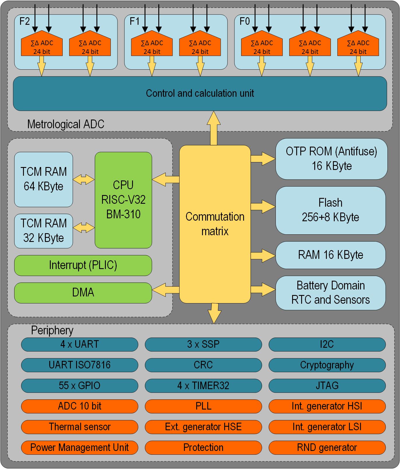
System structure:
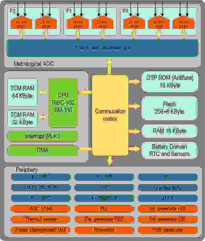
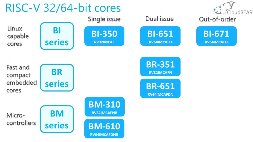
As has been already noted, the heart of a chip is the 32-bit RISC-V processor core (in the RV32 IMC configuration) with BM-310 mark, which has been designed by our good friends from CloudBEAR. It's not their only processor core. They offer a range of cores, from small microcontroller cores to high-performance 64-bit multiprocessor clusters.
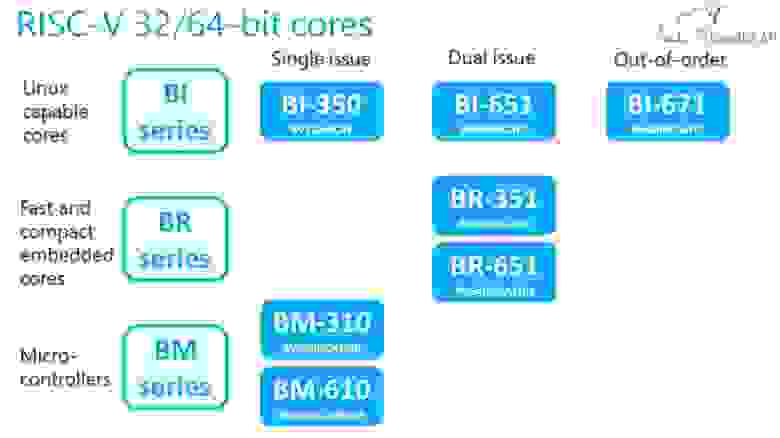
Milandr is developing new products based on cores from different levels of complexity of CloudBEAR portfolio. Only K1986VK025, based on the BM310 core, is available in silicon right now. However, other products, including those based on 64-bit cores, will come out soon. The BM-310 core is a 32-bit RISC-V core with three-staged assembly, with the ability to perform a multiplication operation in two cycles. Floating-point operations support has not been implemented in this version of the chip (although the core allows it to be set up). The performance of the BM-310 core on the CoreMark test is 3.0 CoreMark/MHz. Thus, it can be compared to ARM Cortex-M3. At the same time, the core-area in a new chip is only 0.3 mm2, and considering that most of the tasks of calculating the power consumption parameters are performed by the hardware controller of the metrological ADC, the main processing power of the core can be used for communication tasks in the metering device.
Price is one of the main criteria for the chips. The die-size is the main contributor to the cost of the chip. The larger its area – the more expensive it is, the more complicated technology of production – the more expensive it is either. At the same time, the more complicated technology is used, the smaller area is required to implement the required functionality, and therefore the price can be cheaper. Overall, the choice of technology is not obvious. The first generation K1986BK2x chips were developed at 180 nm. About a third of the die belonged to the analog part (in fact, the sigma-delta ADCs, power supply, IO), and when switching to more subtle processes, this part practically does not decrease. However, in accordance with the new requirements, the amount of functionality should be increased almost 4 times. The new chip implements 256KB Flash against 64K, RAM 112KB against 16K, 5 UART blocks against 2, 3 SPI blocks against 1 and more cryptography… So, after thorough estimations and calculations, it was decided that if you pay special attention to the area, then it is possible to get into the required cost range with 90 nm technologies, with technologies of 65 nm or lower it would be easier, but higher development costs in general would make the project more risky in terms of financing.

As a result, we got a truly compact die, which is more than 2 times smaller in area than the previous one. Although initially there were more ambitious plans to reduce the die to 8 mm2, the result obtained is also very good. Precisely, thanks to this ambition, the shape of the die turned out to be rectangular, and not square. The upper part of the die was given for analog blocks, and its layout was drawn separately for the originally planned dimensions, and when it became clear that the figure would not fit, the die began to «grow» into a rectangle. The same picture took place with the first generation chips. Constancy is a sign of mastery.
If the processor core is the heart of the microcontroller, then the metrological ADC is its brain, since it is the one who specify an assignment of the microcircuit. The microcontroller implements a block of 7 channels of 24 bit ∑∆ ADCs. All channels are divided into three pairs F0-F2 (voltage channel and current channel) for a 3-phase network and one independent current channel (referred to F0). Each of the 7 channels digitizes the input signal with an output sampling rate of up to 16 kHz. Besides, in each pair of channels F0-F2 there is an opportunity to calculate the root-mean-square values of the current / voltage, calculate the active and reactive power, calculate the consumed active and reactive energy, the signal frequency in the voltage channels, the excess of the peak value, and the signal drop below the set level. These additional blocks reduce the load on the processor, which in turn reduces the power consumption of the entire die. In addition, each ADC has an independent DMA channel, providing the ability to save data to RAM without the processor participation.
List of main parameters and capabilities of the sigma-delta ADC unit:
Thus, the main functions of calculating the consumed energy are performed with minimal involvement of the processor.
The microcircuit implements everything to protect information, including:
Symmetric cryptography is implemented on the basis of coprocessors that speed up the most difficult operations. This allows accelerating the encryption speed with top performance up to 10 Mbps. If necessary, asymmetric cryptography algorithms are implemented in software. Overall, one needs to write a separate article about identification, authentication, encryption, and firmware updates, which we will do later on.
In order to prevent various engineering methods of impact both the electricity meter and a separate chip, special engineering protection methods have been implemented:
Pins for tamper detectors are three separate pins of the microcontroller through which signals from external electronic seals are recorded, even in the absence of main-power (only а battery) and when all clocks are off. Thus, any attempts of mechanical impact on the meter will be detected and recorded. In addition to the protection mechanisms of the device case, methods of protecting the microcircuit itself from more sophisticated attacks are implemented.
To eliminate the situation with «acceleration» or vice versa «deceleration» of the processor frequency, a frequency change detector is implemented, which constantly compares the external frequency source with the internal RC generator and, when deviations occur outside the specified limits, it generates the event or switches the chip to an internal (implemented on a chip) emergency frequency source.
«Glitching» of the frequencies signal is countered by the filtering system of the input signal. A voltage detector unit has been implemented for the purpose of correct launch of microcircuits upon turning on the main power supply, as well as detecting the fact that the power supply is outside of acceptable limits. The unit also monitors the charge of the battery level on which the chip operates in the absence of the main power supply. Thus, any manipulations or attempts to break down the operation of the microcircuit through the supply voltages have been eliminated.
To avoid the leakage of key information through «back-side» channels, for example, power circuits, the main power supply noise-masking block has been implemented in the microcircuit using a pseudo-random generator. The block generates a randomly variable additional consumption, masking the main consumption profile.
To prevent more serious semi-invasive and invasive attacks (an attack on a microcircuit when there is access to a die of a microcircuit or even individual circuits of a die), an optical detector has been implemented. Since a die of a microcircuit is usually in the case, light access to it is impossible. In case, a microcircuit is open and light touches a die, the optical sensor will generate an alarm.
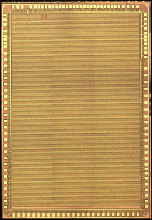
If an intruder has gone even further, then in order to restrict access to the internal circuits of the microcircuit, a protective stack is implemented in the upper layers of the die layout, in which the ground and power circuits are intermingled as well as information circuit along which a random polynomial is transmitted. BTW, this is why the top pictures show a CAD layout drawing, not a real photo of a die.
As for the real picture of a die, it looks like this.
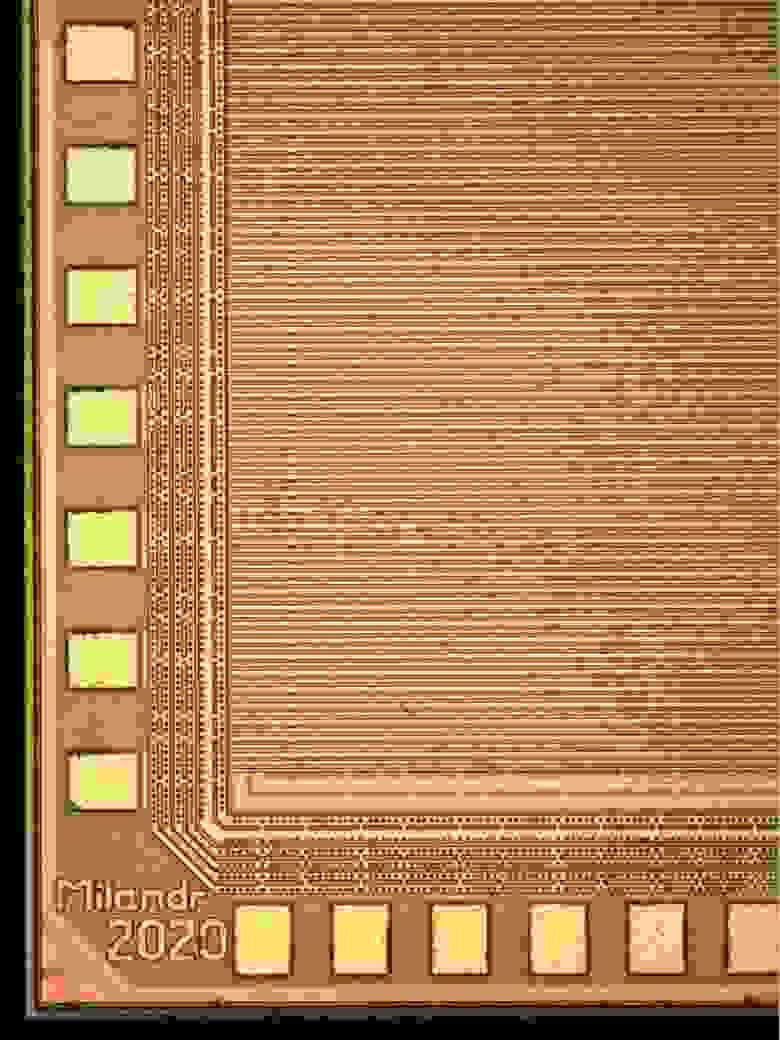
As for a closer look:
For comparison, this is how the security mesh looks like in the ST card chip (ST23 series).

In the event of a physical violation of the mesh integrity, an alarm is generated as well. The software must monitor all alarming events and, if they occur, record the fact of an attack. More to that, microcircuits can be configured so that cryptographic key information is automatically erased when an attack is detected. All this requires the assurance of software.
For the user program, the chip contains 16 Kbytes of one-time programmable ROM (according to the anti-fuse principle) and 256 + 8 Kbytes of reprogrammable Flash. The chip is launched from the built-in one-time programmable memory.
Initially, while chip manufacturing, this memory is clean, and for serial products, the loading of a startup trusted bootloader is to be taken place during testing and rejection. This allows providing a unique identification of each chip, guaranteeing the integrity of the metrological and cryptographic software and is a crucial milestone of trust for the user program as well as ensuring the protection from reading of the user program in Flash.
At time of research for engineering samples, a typical loader for the 1986BE series has been recorded in the startup memory. If necessary, a separate batch of chips can be produced with a startup bootloader adapted to the needs of a consumer.
For initial review of the microcontroller, a demo board has been developed.
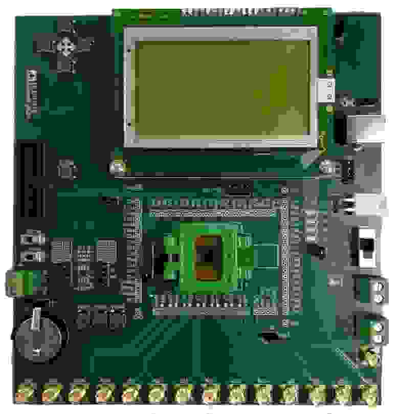
This board is designed for prototyping metering devices; a large number of SMA connectors are designed for connecting metering transformers. This allows not sticking to any specific type of them, and easily connecting precisely those transformers or shunts that are used by the developers of metering devices.
More to that, the absence of high voltage (220V) on the board takes responsibility off us if someone is electrocuted. For larger marketing distribution of the microcircuit, a miniature test board is being developed in the arduino format.
Program development can be carried out in an Eclipce-based environment with a GCC compiler and debugging via OpenOCD, GDB. For debugging in the Eclipse environment, the classic J-Link debuggers and their clones are suitable. Debuggers manufactured by Milandr are also good.
Development can also be carried out in more familiar for many IAR Embedded Workbench environment, which includes debugging, compilation and optimization tools. For debugging, either the signature I-JET for RISC-V lanyard is used or, if you order the Evaluation Kit for RISC-V, you will also receive an I-jet Lite debug probe (which also supported by ARM), as well as 30 day license for environment itself.
Yesterday's bold ideas, today are being embodied in technical solutions and are becoming the standard practice. The world in which we are living does not allow us standing still. The creation of the chip described above has a huge impact on the entire RISC-V community. I congratulate all those involved in the development of this chip with its birth. Also, I hope that consumers (developers of metering devices) will take it positively, and despite the skepticism towards Russian chips, I am sure we can compete with foreign companies.
Welcome to RISC-V era!
Spacial thanks for Stasevich Olga.
Solutions based on the open standard instruction set architecture RISC-V are currently increasing their presence on the market. Microcontrollers from Chinese colleagues are already in serial production; Microchip is offering interesting solutions with FPGA on board. The ecosystem of software and design tools for this architecture are also growing. Seeming previously unshaken leaders have more often found themselves in resale ads, while young startups attract multi-million investments. Milandr also got involved in this race and today began supplying interested companies with samples of its new K1986BK025 microcontroller based on the RISC-V processor core for electricity meters. Well here we go, pictures, characteristics and other information, as well as a little bit of hype under the cut.
What is the RISC-V? Hail to the Great Habr and its users, who have already written many articles on this topic, and spare me from this fate. Look at RRISC-V from scratch. You can also get familiar with the series products from GigaDevice, as well as criticism and cons description of RISC-V architecture from ARM employees.
The K1986BK025 microcontroller based on the RISC-V core is the second generation of Milandr’s microcontrollers for electricity meters. The first generation — K1986BK2x chip has been developed on ARM Cortex-M0 processor core and produced for more than 5 years. On their basis, Milur meters have now being designed.
Nevertheless, time never stands still and new market rules dictate new requirements for new chips. More functions need to be introduced — new requirements for the «minimum functionality» of metering devices (Russian standrts). You need to fit into required price, as you will have to compete with monsters like TI and NXP. Besides, if you follow this direction, you know that new «smart» electricity meters can turn off electricity limit electricity consumption. That means a new system should provide information security as well, so that intruders would not be able to turn off or turn on the electricity at their discretion. All of this has resulted in a new chip K1986BK025, which we are now going to talk about.
1. Main feathures К1986ВК025
Processor core — RISC-V (BМ-310S CloudBEAR)
Frequency — 60 MHz
Supply voltage (main) 2,2...3,6 V
Supply voltage (ADC uses) 3,0...3,6 V
Supply voltage (battery-operated) 1,8...3,6 V
Flash program memory capacity — 256+8 Kbyte
Memory capacity RAM — 112 Kbyte
Capacity of one time programmable ROM — 16 Kbyte
Metrological electicity measuring ADC — 24-bit sigma delta, 7 channels
Hardware unit for calculating power consumption
Instrumental ADC – 10 bits with temperature sensor
Interfaces — 5xUART, 3xSPI, 1xI2C
User IO — 55
512-byte battery domain with real-time clock and tamper detection
4 32-bit timer blocks with 4 Event Capture channels and PWM
Watchdog Timer
CRC count block with variable polynomial
Symmetric cryptographic algorithm calculation support block
Random Number Generator Unit
Frequency Change Detector Unit
Supply Voltage Detector Unit (main and battery)
Optical detector block
Noise generation unit in power supply chain
Shield Screen Grid
Debug Interface — JTAG
Package Type — QFN88 (10 x 10 mm)
Operating temperature -50°C… +85°C
System structure:
2. Processor core
As has been already noted, the heart of a chip is the 32-bit RISC-V processor core (in the RV32 IMC configuration) with BM-310 mark, which has been designed by our good friends from CloudBEAR. It's not their only processor core. They offer a range of cores, from small microcontroller cores to high-performance 64-bit multiprocessor clusters.
Milandr is developing new products based on cores from different levels of complexity of CloudBEAR portfolio. Only K1986VK025, based on the BM310 core, is available in silicon right now. However, other products, including those based on 64-bit cores, will come out soon. The BM-310 core is a 32-bit RISC-V core with three-staged assembly, with the ability to perform a multiplication operation in two cycles. Floating-point operations support has not been implemented in this version of the chip (although the core allows it to be set up). The performance of the BM-310 core on the CoreMark test is 3.0 CoreMark/MHz. Thus, it can be compared to ARM Cortex-M3. At the same time, the core-area in a new chip is only 0.3 mm2, and considering that most of the tasks of calculating the power consumption parameters are performed by the hardware controller of the metrological ADC, the main processing power of the core can be used for communication tasks in the metering device.
3. Price
Price is one of the main criteria for the chips. The die-size is the main contributor to the cost of the chip. The larger its area – the more expensive it is, the more complicated technology of production – the more expensive it is either. At the same time, the more complicated technology is used, the smaller area is required to implement the required functionality, and therefore the price can be cheaper. Overall, the choice of technology is not obvious. The first generation K1986BK2x chips were developed at 180 nm. About a third of the die belonged to the analog part (in fact, the sigma-delta ADCs, power supply, IO), and when switching to more subtle processes, this part practically does not decrease. However, in accordance with the new requirements, the amount of functionality should be increased almost 4 times. The new chip implements 256KB Flash against 64K, RAM 112KB against 16K, 5 UART blocks against 2, 3 SPI blocks against 1 and more cryptography… So, after thorough estimations and calculations, it was decided that if you pay special attention to the area, then it is possible to get into the required cost range with 90 nm technologies, with technologies of 65 nm or lower it would be easier, but higher development costs in general would make the project more risky in terms of financing.
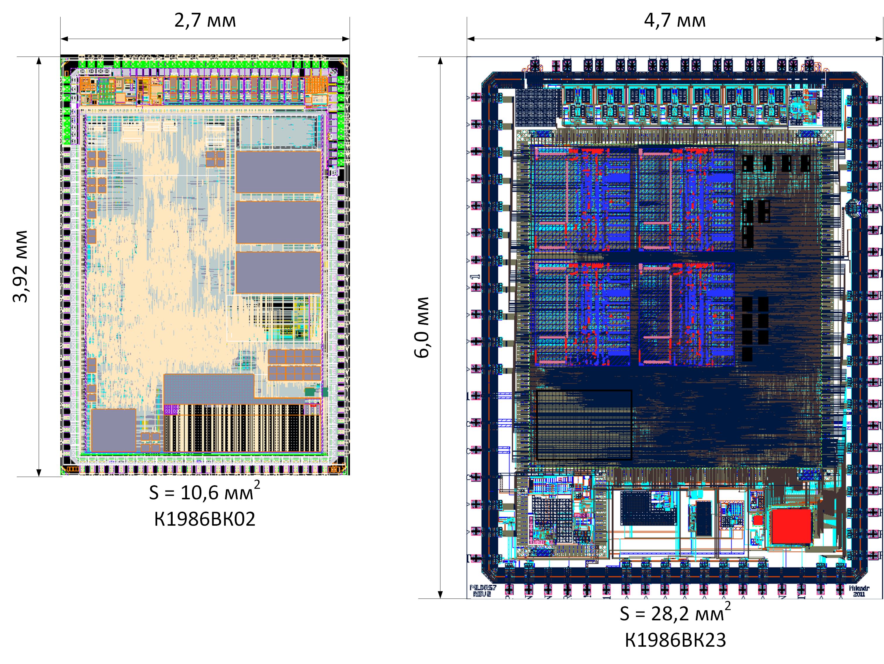
As a result, we got a truly compact die, which is more than 2 times smaller in area than the previous one. Although initially there were more ambitious plans to reduce the die to 8 mm2, the result obtained is also very good. Precisely, thanks to this ambition, the shape of the die turned out to be rectangular, and not square. The upper part of the die was given for analog blocks, and its layout was drawn separately for the originally planned dimensions, and when it became clear that the figure would not fit, the die began to «grow» into a rectangle. The same picture took place with the first generation chips. Constancy is a sign of mastery.
4. Metrological ADC
If the processor core is the heart of the microcontroller, then the metrological ADC is its brain, since it is the one who specify an assignment of the microcircuit. The microcontroller implements a block of 7 channels of 24 bit ∑∆ ADCs. All channels are divided into three pairs F0-F2 (voltage channel and current channel) for a 3-phase network and one independent current channel (referred to F0). Each of the 7 channels digitizes the input signal with an output sampling rate of up to 16 kHz. Besides, in each pair of channels F0-F2 there is an opportunity to calculate the root-mean-square values of the current / voltage, calculate the active and reactive power, calculate the consumed active and reactive energy, the signal frequency in the voltage channels, the excess of the peak value, and the signal drop below the set level. These additional blocks reduce the load on the processor, which in turn reduces the power consumption of the entire die. In addition, each ADC has an independent DMA channel, providing the ability to save data to RAM without the processor participation.
List of main parameters and capabilities of the sigma-delta ADC unit:
- 7 independent ADCs with an output sample rate of 4/8/16 kHz (4 current channels and 3 voltage channels). These channels make up 3 blocks for measuring the parameters of each phase F0-F2.
- In the block of channels F0, we implement automatic selection of the current channel (which has the maximum value) for subsequent calculations of the power characteristics. If the current difference exceeds 6%, an interruption is generated. Apart from this function, the rest of the blocks F0-F2 are identical.
- All ADC channels have independent slope calibration coefficients characteristics.
- Each current channel has an independent integrator.
- Each ADC block (F0-F2) independently calculates the signal period via the voltage channel. The number of periods during which this value is calculated may be set equal to 1/2/4/8/16/32/64/128 periods.
- Each block is able to verify the loss of a periodic signal in the voltage channel.
- Each block is able to verify the voltage “drop” below the specified level, as well as the excess of the signal in the current and voltage channels over the specified limit.
- It allows correcting the phase of the signals in the voltage channels with an accuracy of 0.02%.
- It allows calculating root mean square values, squared root mean square values of currents and voltages, as well as their independent calibration.
- When calculating active and reactive energy, the value of the accumulated energy during the period is stored in separate registers (for positive and negative energy).
- Full power and full energy are calculated.
- The phase shift is calculated with respect to phase 0.
Thus, the main functions of calculating the consumed energy are performed with minimal involvement of the processor.
5. Protection
5.1. Cryptography
The microcircuit implements everything to protect information, including:
- Blocks of coprocessors to support block ciphers AES;
- Block of the random number generator;
- Block for calculating CRC for an arbitrary polynomial;
- Block of special volatile memory of key information with battery
- One-time programmable bootloader ROM that implements the unique identification of each chip.
Symmetric cryptography is implemented on the basis of coprocessors that speed up the most difficult operations. This allows accelerating the encryption speed with top performance up to 10 Mbps. If necessary, asymmetric cryptography algorithms are implemented in software. Overall, one needs to write a separate article about identification, authentication, encryption, and firmware updates, which we will do later on.
5.2. Engineering protection
In order to prevent various engineering methods of impact both the electricity meter and a separate chip, special engineering protection methods have been implemented:
- 3 pins for tamper detectors (electronic seals)
- Block of the detector of frequency change
- Supply voltage change detector unit
- Optical detector unit
- Block generating noise in the power supply circuit
- Protective screen mesh
- Protection against unauthorized memory reading
Pins for tamper detectors are three separate pins of the microcontroller through which signals from external electronic seals are recorded, even in the absence of main-power (only а battery) and when all clocks are off. Thus, any attempts of mechanical impact on the meter will be detected and recorded. In addition to the protection mechanisms of the device case, methods of protecting the microcircuit itself from more sophisticated attacks are implemented.
To eliminate the situation with «acceleration» or vice versa «deceleration» of the processor frequency, a frequency change detector is implemented, which constantly compares the external frequency source with the internal RC generator and, when deviations occur outside the specified limits, it generates the event or switches the chip to an internal (implemented on a chip) emergency frequency source.
«Glitching» of the frequencies signal is countered by the filtering system of the input signal. A voltage detector unit has been implemented for the purpose of correct launch of microcircuits upon turning on the main power supply, as well as detecting the fact that the power supply is outside of acceptable limits. The unit also monitors the charge of the battery level on which the chip operates in the absence of the main power supply. Thus, any manipulations or attempts to break down the operation of the microcircuit through the supply voltages have been eliminated.
To avoid the leakage of key information through «back-side» channels, for example, power circuits, the main power supply noise-masking block has been implemented in the microcircuit using a pseudo-random generator. The block generates a randomly variable additional consumption, masking the main consumption profile.
To prevent more serious semi-invasive and invasive attacks (an attack on a microcircuit when there is access to a die of a microcircuit or even individual circuits of a die), an optical detector has been implemented. Since a die of a microcircuit is usually in the case, light access to it is impossible. In case, a microcircuit is open and light touches a die, the optical sensor will generate an alarm.
If an intruder has gone even further, then in order to restrict access to the internal circuits of the microcircuit, a protective stack is implemented in the upper layers of the die layout, in which the ground and power circuits are intermingled as well as information circuit along which a random polynomial is transmitted. BTW, this is why the top pictures show a CAD layout drawing, not a real photo of a die.
As for the real picture of a die, it looks like this.

As for a closer look:
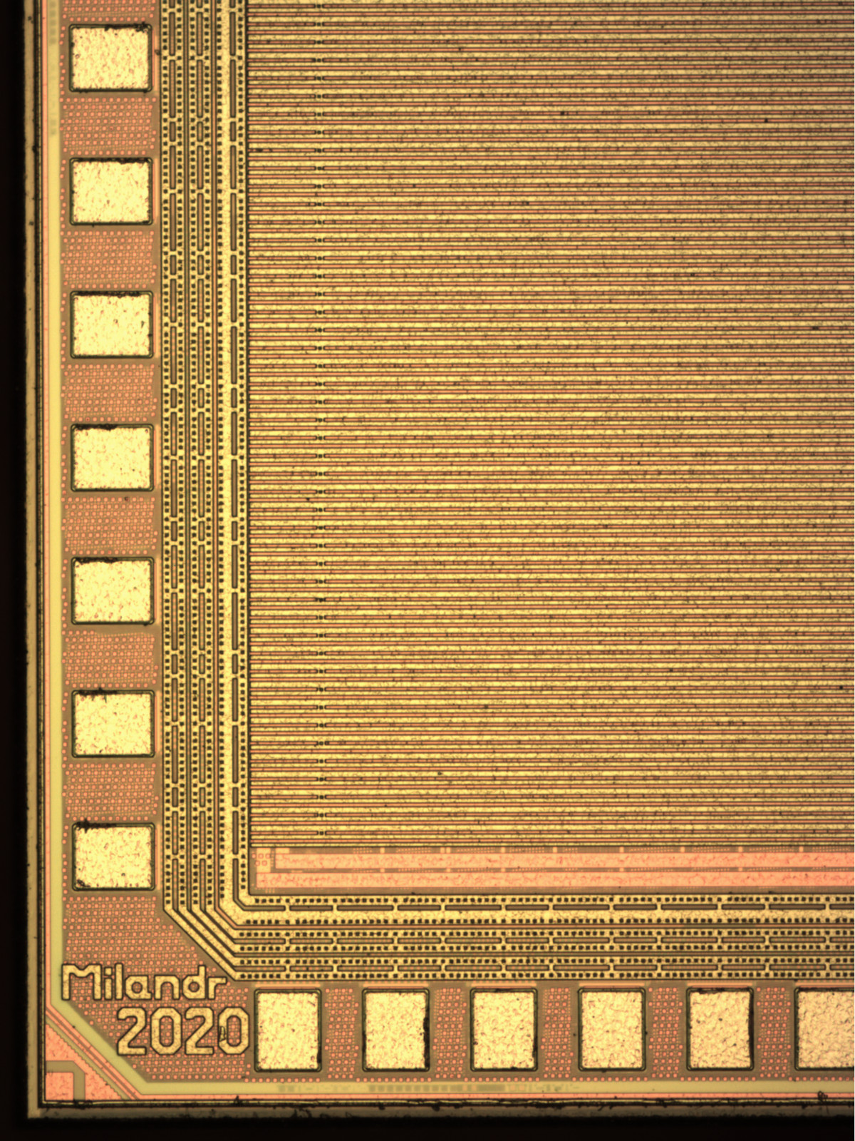
For comparison, this is how the security mesh looks like in the ST card chip (ST23 series).

In the event of a physical violation of the mesh integrity, an alarm is generated as well. The software must monitor all alarming events and, if they occur, record the fact of an attack. More to that, microcircuits can be configured so that cryptographic key information is automatically erased when an attack is detected. All this requires the assurance of software.
For the user program, the chip contains 16 Kbytes of one-time programmable ROM (according to the anti-fuse principle) and 256 + 8 Kbytes of reprogrammable Flash. The chip is launched from the built-in one-time programmable memory.
Initially, while chip manufacturing, this memory is clean, and for serial products, the loading of a startup trusted bootloader is to be taken place during testing and rejection. This allows providing a unique identification of each chip, guaranteeing the integrity of the metrological and cryptographic software and is a crucial milestone of trust for the user program as well as ensuring the protection from reading of the user program in Flash.
At time of research for engineering samples, a typical loader for the 1986BE series has been recorded in the startup memory. If necessary, a separate batch of chips can be produced with a startup bootloader adapted to the needs of a consumer.
6. Design tools
For initial review of the microcontroller, a demo board has been developed.
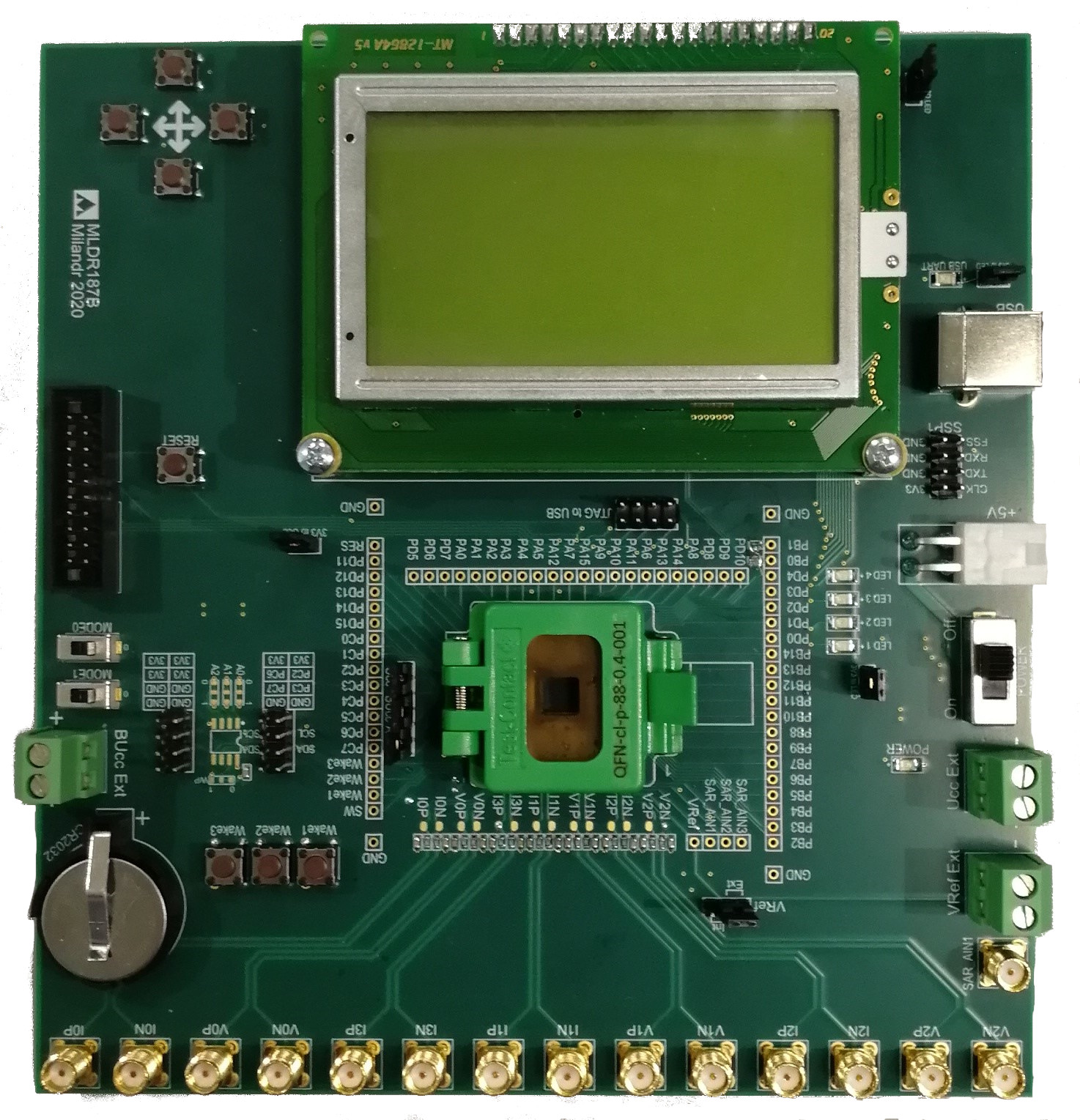
This board is designed for prototyping metering devices; a large number of SMA connectors are designed for connecting metering transformers. This allows not sticking to any specific type of them, and easily connecting precisely those transformers or shunts that are used by the developers of metering devices.
More to that, the absence of high voltage (220V) on the board takes responsibility off us if someone is electrocuted. For larger marketing distribution of the microcircuit, a miniature test board is being developed in the arduino format.
6.1. Eclipse+GCC
Program development can be carried out in an Eclipce-based environment with a GCC compiler and debugging via OpenOCD, GDB. For debugging in the Eclipse environment, the classic J-Link debuggers and their clones are suitable. Debuggers manufactured by Milandr are also good.
6.2. IAR
Development can also be carried out in more familiar for many IAR Embedded Workbench environment, which includes debugging, compilation and optimization tools. For debugging, either the signature I-JET for RISC-V lanyard is used or, if you order the Evaluation Kit for RISC-V, you will also receive an I-jet Lite debug probe (which also supported by ARM), as well as 30 day license for environment itself.
Conclusion
Yesterday's bold ideas, today are being embodied in technical solutions and are becoming the standard practice. The world in which we are living does not allow us standing still. The creation of the chip described above has a huge impact on the entire RISC-V community. I congratulate all those involved in the development of this chip with its birth. Also, I hope that consumers (developers of metering devices) will take it positively, and despite the skepticism towards Russian chips, I am sure we can compete with foreign companies.
Welcome to RISC-V era!
Spacial thanks for Stasevich Olga.
